MICRF505DEV1 Micrel Inc, MICRF505DEV1 Datasheet - Page 9
MICRF505DEV1
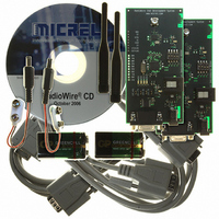
Manufacturer Part Number
MICRF505DEV1
Description
KIT DEV RADIOWIRE 850-950MHZ
Manufacturer
Micrel Inc
Series
RadioWire®r
Type
Transceiver, ISMr
Specifications of MICRF505DEV1
Frequency
850MHz ~ 950MHz
For Use With/related Products
MICRF505
Lead Free Status / RoHS Status
Lead free / RoHS Compliant
Other names
576-1606
Available stocks
Company
Part Number
Manufacturer
Quantity
Price
Company:

Part Number:
MICRF505DEV1
Manufacturer:
Micrel Inc
Quantity:
135


0000000
0000001
0000010
0000011
0000100
0000101
0000110
0000111
0001000
0001001
0001010
0001011
0001100
0001101
0001110
0001111
0010000
0010001
0010010
0010011
0010100
0010101
0010110
A6…A0
Programming
General
The MICRF505 functions are enabled through a
number of programming bits. The programming bits
are organized as a set of addressable control
registers, each register holding 8 bits.
There are 23 control registers in total in the
MICRF505, and they have addresses ranging from 0
to 22. The user can read all the control registers.
The user can write to the first 22 registers (0 to 21);
the register 22 is a read-only register.
All control registers hold 8 bits and all 8 bits must be
written to when accessing a control register, or they
will be read. Some of the registers do not utilize all 8
bits. The value of an unused bit is “don’t care.”
The control register with address 0 is referred to as
ControlRegister0, the control register with address 1
is ControlRegister1 and so on. A summary of the
control registers is given in the table below. In
addition to the unused bits (marked with”-“) there are
a number of mandatory bits (marked with “0” or “1”).
Always maintain these as shown in the table.
Adr
October 2006
Names of programming bits, unused bits (“-“) and mandatory bits (“1” or “0”) are shown. Change of mandatory bits may cause malfunction.
BitRate_clkS1
Modulation1
Mod_F2
LNA_by
CP_HI
FEE_7
N0_7
M0_7
N1_7
M1_7
D7
‘1’
‘1’
‘0’
‘1’
-
-
-
-
-
-
-
-
-
BitRate_clkS0
Modulation0
Mod_clkS2
Mod_F1
FEE_6
SC_by
M0_6
M1_6
N0_6
N1_6
PA2
D6
‘1’
‘1’
‘0’
‘0’
-
-
-
-
-
-
-
-
Mod_clkS1
RefClk_K5
Table 1. Control Registers in MICRF505
Mod_F0
ScClk5
FEE_5
M0_5
M1_5
A0_5
N0_5
A1_5
N1_5
PA1
D5
‘0’
‘0’
‘0’
‘0’
‘1’
‘1’
-
-
-
-
-
Mod_clkS0
RefClk_K4
XCOtune4
VCO_IB2
Mod_I4
ScClk4
PA_By
FEE_4
M0_4
M1_4
A0_4
N0_4
A1_4
N1_4
PA0
D4
‘0’
‘1’
‘1’
-
-
-
-
-
9
Data
BitSync_clkS2
The control registers in MICRF505 are accessed
through a 3-wire interface; clock, data and chip
select. These lines are referred to as SCLK, IO, and
CS, respectively. This 3-wire interface is dedicated
to control register access and is referred to as the
control interface. Received data (via RF) and data to
transmit (via RF) are handled by the DataIXO and
DataClk (if enabled) lines; this is referred to as the
data interface.
The SCLK line is applied externally; access to the
control registers are carried out at a rate determined
by the user. The MICRF505 will ignore transitions on
the SCLK line if the CS line is inactive. The
MICRF505 can be put on a bus, sharing clock and
data lines with other devices.
All control registers should be written to after a
battery reset. During operation, it is sufficient to write
to
automatically enter power down mode after a battery
reset.
RefClk_K3
XCOtune3
VCO_IB1
Sync_en
RSSI_en
FEEC_3
Mod_A3
OUTS3
Mod_I3
ScClk3
M0_11
M1_11
FEE_3
N0_11
N1_11
M0_3
M1_3
A0_3
N0_3
A1_3
N1_3
D3
one
‘0’
register
BitSync_clkS1
RefClk_K2
XCOtune2
VCO_IB0
Mod_A2
FEEC_2
OUTS2
Mod_I2
ScClk2
Mode1
N0_10
M0_10
N1_10
M1_10
FEE_2
LD_en
N0_2
M0_2
N1_2
M1_2
A0_2
A1_2
D2
‘1’
only.
BitSync_clkS0
The
VCO_freq1
RefClk_K1
XCOtune1
FEEC_1
PF_FC1
Mod_A1
Mod_I1
OUTS1
ScClk1
Mode0
FEE_1
M0_9
M0_1
M1_9
M1_1
A0_1
N0_9
N0_1
A1_1
N1_9
N1_1
D1
‘0’
MICRF505
+1 408-944-0800
M9999-103106
BitRate_clkS2
VCO_freq0
RefClk_K0
XCOtune0
Load_en
PF_FC0
Mod_A0
FEEC_0
OUTS0
Mod_I0
ScClk0
FEE_0
M0_8
M0_0
M1_8
M1_0
A0_0
N0_8
N0_0
A1_0
N1_8
N1_0
D0
‘1’
will
Related parts for MICRF505DEV1
Image
Part Number
Description
Manufacturer
Datasheet
Request
R

Part Number:
Description:
Manufacturer:
Micrel Inc
Datasheet:
Part Number:
Description:
Manufacturer:
Micrel Inc
Datasheet:
Part Number:
Description:
Manufacturer:
Micrel Inc
Datasheet:
Part Number:
Description:
Manufacturer:
Micrel Inc
Datasheet:
Part Number:
Description:
Manufacturer:
Micrel Inc
Datasheet:
Part Number:
Description:
Manufacturer:
Micrel Inc
Datasheet:
Part Number:
Description:
Manufacturer:
Micrel Inc
Datasheet:
Part Number:
Description:
Manufacturer:
Micrel Inc
Datasheet:
Part Number:
Description:
Manufacturer:
Micrel Inc
Datasheet:
Part Number:
Description:
Manufacturer:
Micrel Inc
Datasheet:
Part Number:
Description:
Manufacturer:
Micrel Inc
Datasheet:
Part Number:
Description:
Manufacturer:
Micrel Inc
Datasheet:
Part Number:
Description:
Manufacturer:
Micrel Inc
Datasheet:
Part Number:
Description:
Manufacturer:
Micrel Inc
Datasheet: