1320X-QE-DSK-BDM Freescale Semiconductor, 1320X-QE-DSK-BDM Datasheet - Page 39
1320X-QE-DSK-BDM
Manufacturer Part Number
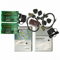
1320X-QE-DSK-BDM
Description
KIT EVAL FOR MC1320X BDM CABLE
Manufacturer
Freescale Semiconductor
Type
Transceiver, 802.15.4/ZigBeer
Specifications of 1320X-QE-DSK-BDM
Frequency
2.4GHz
Interface Type
USB
For Use With/related Products
MC1320x
Lead Free Status / RoHS Status
Lead free / RoHS Compliant


6.3
The PCB composite materials must meet the following requirements:
6.4
The solder mask must meet the following requirements:
6.5
The silk screen must meet the following requirements:
6.6
6.7
Packaging for the PCBs must be the following requirements:
Freescale Semiconductor
•
•
•
•
•
•
•
•
•
•
•
•
•
Laminate - The base laminate material (laminate) must be FR4. If the laminate material were
changed the RF electrical characteristics may change and degrade RF performance. Interior
dielectric thickness is 1.02 mm (40 mils) and the outer dielectric thickness is 0.254 mm (10 mils).
Copper Foil -
— Top and Bottom copper layers must be 1 oz. copper
— Interior layers must be 1/2 oz. copper
Plating - All pad plating must be Hot Air Levelling (HAL)
Solder mask type: Liquid Film Electra EMP110 or equivalent
Solder mask thickness: 10 – 30 µm
Silkscreen color: White
Silkscreen must be applied after application of solder mask if solder mask is required
The silkscreen ink must not extend into any plated-thru-holes
The silk screen must be clipped back to the line of resistance
All PCBs must be 100 percent tested for opens and shorts
Impedance Measurement - An impedance measurement report is not mandatory
Finished PCBs must remain in panel
Finished PCBs must be packed in plastic bags that do not contain silicones or sulphur materials.
These materials can degrade solderability.
Materials
Solder Mask
Silk Screen
Electrical PCB Testing
Packaging
1320x-QE128EVB Reference Manual, Rev. 1.0
PCB Manufacturing Specifications
6-3
Related parts for 1320X-QE-DSK-BDM
Image
Part Number
Description
Manufacturer
Datasheet
Request
R

Part Number:
Description:
KIT DEV FOR MC1320X QE RFIC
Manufacturer:
Freescale Semiconductor
Datasheet:

Part Number:
Description:
Manufacturer:
Freescale Semiconductor, Inc
Datasheet:
Part Number:
Description:
Manufacturer:
Freescale Semiconductor, Inc
Datasheet:
Part Number:
Description:
Manufacturer:
Freescale Semiconductor, Inc
Datasheet:
Part Number:
Description:
Manufacturer:
Freescale Semiconductor, Inc
Datasheet:
Part Number:
Description:
Manufacturer:
Freescale Semiconductor, Inc
Datasheet:
Part Number:
Description:
Manufacturer:
Freescale Semiconductor, Inc
Datasheet:
Part Number:
Description:
Manufacturer:
Freescale Semiconductor, Inc
Datasheet:
Part Number:
Description:
Manufacturer:
Freescale Semiconductor, Inc
Datasheet:
Part Number:
Description:
Manufacturer:
Freescale Semiconductor, Inc
Datasheet:
Part Number:
Description:
Manufacturer:
Freescale Semiconductor, Inc
Datasheet:
Part Number:
Description:
Manufacturer:
Freescale Semiconductor, Inc
Datasheet:
Part Number:
Description:
Manufacturer:
Freescale Semiconductor, Inc
Datasheet:
Part Number:
Description:
Manufacturer:
Freescale Semiconductor, Inc
Datasheet:
Part Number:
Description:
Manufacturer:
Freescale Semiconductor, Inc
Datasheet: