ATAKSTK511-8 Atmel, ATAKSTK511-8 Datasheet - Page 24
ATAKSTK511-8
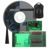
Manufacturer Part Number
ATAKSTK511-8
Description
KIT RF MODULE 868MHZ FOR STK500
Manufacturer
Atmel
Series
SmartRF®r
Type
Transmitter, Receiver, ASK, FSKr
Specifications of ATAKSTK511-8
Frequency
868MHz
Wireless Frequency
868 MHz
For Use With/related Products
ATSTK500
Lead Free Status / RoHS Status
Contains lead / RoHS non-compliant


1925C–AVR–3/03
Hardware Description
3.7.2.2
3-14
Serial High-voltage
Programming
The 8-pin AVRs have too few pins to use parallel communication during High-voltage
Programming. They use serial communication instead.
This means that fewer signals have to be routed. Hardware setup for serial High-voltage
Programming is as follows:
1. Switch power off.
2. Place the device to program in its socket according to Table 3-3 on page 3-11.
3. Mount jumper OSCSEL on pins 1 and 2 to select software-controlled clock.
4. Mount jumper XTAL1 to route the oscillator signal to the device.
5. Mount jumpers VTARGET and RESET.
6. Use one 2-wire cable to connect the PB3 pin (pin 4) on the PORTB header to the
7. Use another 2-wire cable to connect the PB5 pin (pin 6) on the PORTB header to
8. Use a third 2-wire cable to connect the PB0 and PB2 pins (pins 4 and 3) on the
9. Use the last 2-wire cable to connect the PB1 pin (pin 1) on the SPROG1 header
10. Switch power on and you are ready to program.
All connections are shown in Figure 3-19.
Figure 3-19. Connection for Serial High-voltage Programming
XT1 pin (pin 7) on the PORTE/AUX header. This will connect the clock system to
the AVR device.
the RST pin (pin 4) on the PORTE/AUX header. This will connect the reset sys-
tem to the AVR device.
SPROG1 header to the DATA0 and DATA2 pins (pins 1 and 3) on the PROG
DATA header.
to the DATA1 pin (pin 2) on the PROG DATA header.
AVR STK500 User Guide
Related parts for ATAKSTK511-8
Image
Part Number
Description
Manufacturer
Datasheet
Request
R

Part Number:
Description:
DEV KIT FOR AVR/AVR32
Manufacturer:
Atmel
Datasheet:

Part Number:
Description:
INTERVAL AND WIPE/WASH WIPER CONTROL IC WITH DELAY
Manufacturer:
ATMEL Corporation
Datasheet:
Part Number:
Description:
Low-Voltage Voice-Switched IC for Hands-Free Operation
Manufacturer:
ATMEL Corporation
Datasheet:
Part Number:
Description:
MONOLITHIC INTEGRATED FEATUREPHONE CIRCUIT
Manufacturer:
ATMEL Corporation
Datasheet:
Part Number:
Description:
AM-FM Receiver IC U4255BM-M
Manufacturer:
ATMEL Corporation
Datasheet:
Part Number:
Description:
Monolithic Integrated Feature Phone Circuit
Manufacturer:
ATMEL Corporation
Datasheet:
Part Number:
Description:
Multistandard Video-IF and Quasi Parallel Sound Processing
Manufacturer:
ATMEL Corporation
Datasheet:
Part Number:
Description:
High-performance EE PLD
Manufacturer:
ATMEL Corporation
Datasheet:
Part Number:
Description:
8-bit Flash Microcontroller
Manufacturer:
ATMEL Corporation
Datasheet:
Part Number:
Description:
2-Wire Serial EEPROM
Manufacturer:
ATMEL Corporation
Datasheet: