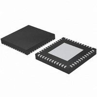
TDA9898HN/V2,551 NXP Semiconductors, TDA9898HN/V2,551 Datasheet - Page 62

TDA9898HN/V2,551
Manufacturer Part Number
TDA9898HN/V2,551
Description
IC IF PROCESSOR MULTISTD 48HVQFN
Manufacturer
NXP Semiconductors
Datasheet
1.TDA9898HNV3518.pdf
(103 pages)
Specifications of TDA9898HN/V2,551
Function
IF Processor
Rf Type
ATV, DVB, FM
Package / Case
48-VFQFN Exposed Pad
Lead Free Status / RoHS Status
Lead free / RoHS Compliant
Other names
935283079551
TDA9898HN/V2-S
TDA9898HN/V2-S
TDA9898HN/V2-S
TDA9898HN/V2-S
- Current page: 62 of 103
- Download datasheet (530Kb)
NXP Semiconductors
Table 53.
V
f
for L); IF input from 50
B/G is 10 % and for L is 3 %; video signal in accordance with “ITU-T J.63 line 17 and line 330” or “NTC-7 Composite”;
internal Nyquist slope switched on (W7[0] = 0); measurements taken in test circuit of
[1]
[2]
[3]
[4]
TDA9897_TDA9898_4
Product data sheet
Symbol
V
I
V
V
I
I
V
f
Pins PORT1 or PORT2 or PORT3 operating as open-collector output port
V
I
V
SC
2
IH
IL
SCL
sink(o)
P
I
C-bus transceiver; pins SCL and SDA
IH
IL
OL
OL
OH
= 5 V; T
= 32.875 MHz; PC / SC = 13 dB; f
Values of video and sound parameters can be decreased at V
Condition for secure POR is a rise or fall time greater than 2 s.
This parameter is not tested during the production and is only given as application information for designing the receiver circuit.
Level headroom for input level jumps during gain control setting.
amb
Characteristics
= 25 C; see
Parameter
input voltage
HIGH-level input voltage
LOW-level input voltage
HIGH-level input current
LOW-level input current
LOW-level output voltage
SCL clock frequency
LOW-level output voltage
output sink current
HIGH-level output voltage
via broadband transformer 1 : 1; video modulation: Vestigial SideBand (VSB); residual carrier for
Table 24
…continued
for input frequencies; B/G standard is used for the specification (f
AF
[31]
= 400 Hz); input level V
Conditions
V
pin connected to V
V
pin open-circuit
V
pin connected to GND
V
V
V
V
V
V
I
transmission (SDA)
I = 2 mA (sink)
PORT1
PORT2; W8[7] = 1
PORT3; W8[7] = 1
OL
CC(I2C-bus)
CC(I2C-bus)
CC(I2C-bus)
CC(I2C-bus)
CC(I2C-bus)
CC(I2C-bus)
CC(I2C-bus)
CC(I2C-bus)
CC(I2C-bus)
W7[3] = 0
W7[3] = 1
W8[1] = 0
W8[1] = 1
W8[2] = 0
W8[2] = 1
Rev. 04 — 25 May 2009
= 3 mA; for data
= 5.0 V;
= 3.3 V;
= 2.5 V;
= 5.0 V
= 3.3 V
= 2.5 V
= 5.0 V
= 3.3 V
= 2.5 V
P
= 4.5 V.
i(IF)
P
= 10 mV (RMS) (sync level for B/G; peak white level
TDA9897; TDA9898
[32]
[33]
[33]
[32]
[33]
[33]
Multistandard hybrid IF processing
Min
0.88V
0.46V
0
0.6V
2.3
1.75
-
0
-
-
-
-
-
-
-
-
Figure
0.3
0.3
0.3
10
10
P
P
P
51; unless otherwise specified.
Typ
-
-
-
-
-
-
-
-
-
-
-
-
-
-
-
-
-
-
-
-
-
PC
© NXP B.V. 2009. All rights reserved.
= 38.375 MHz;
Max
V
0.58V
0.12V
V
V
V
+0.3V
+1.0
+0.75
+10
+10
0.4
400
0.4
3
10
3
10
3
10
V
P
P
P
P
P
+ 0.5 V
P
P
P
Unit
V
V
V
V
V
V
V
V
V
V
kHz
V
mA
mA
mA
62 of 103
A
A
A
A
A
Related parts for TDA9898HN/V2,551
Image
Part Number
Description
Manufacturer
Datasheet
Request
R

Part Number:
Description:
IC IF PROCESSOR MULTISTD 48HVQFN
Manufacturer:
NXP Semiconductors
Datasheet:
Part Number:
Description:
Up-Down Converters MULTI APPL SYS FOR TERRESTR IF
Manufacturer:
NXP Semiconductors
Part Number:
Description:
Up-Down Converters MULTI APPL SYS FOR TERRESTR IF
Manufacturer:
NXP Semiconductors

Part Number:
Description:
IC IF PROCESSOR HYBRID 48-HVQFN
Manufacturer:
NXP Semiconductors
Datasheet:

Part Number:
Description:
IC IF PROCESSOR HYBRID 48-HVQFN
Manufacturer:
NXP Semiconductors
Datasheet:

Part Number:
Description:
IC IF PROCESSOR HYBRID 48-HVQFN
Manufacturer:
NXP Semiconductors
Datasheet:
Part Number:
Description:
Tda9897; Tda9898 Multistandard Hybrid If Processing
Manufacturer:
NXP Semiconductors
Datasheet:
Part Number:
Description:
Multistandard Hybrid If Processing Semiconductors
Manufacturer:
NXP Semiconductors
Datasheet:
Part Number:
Description:
NXP Semiconductors designed the LPC2420/2460 microcontroller around a 16-bit/32-bitARM7TDMI-S CPU core with real-time debug interfaces that include both JTAG andembedded trace
Manufacturer:
NXP Semiconductors
Datasheet:

Part Number:
Description:
NXP Semiconductors designed the LPC2458 microcontroller around a 16-bit/32-bitARM7TDMI-S CPU core with real-time debug interfaces that include both JTAG andembedded trace
Manufacturer:
NXP Semiconductors
Datasheet:
Part Number:
Description:
NXP Semiconductors designed the LPC2468 microcontroller around a 16-bit/32-bitARM7TDMI-S CPU core with real-time debug interfaces that include both JTAG andembedded trace
Manufacturer:
NXP Semiconductors
Datasheet:
Part Number:
Description:
NXP Semiconductors designed the LPC2470 microcontroller, powered by theARM7TDMI-S core, to be a highly integrated microcontroller for a wide range ofapplications that require advanced communications and high quality graphic displays
Manufacturer:
NXP Semiconductors
Datasheet:
Part Number:
Description:
NXP Semiconductors designed the LPC2478 microcontroller, powered by theARM7TDMI-S core, to be a highly integrated microcontroller for a wide range ofapplications that require advanced communications and high quality graphic displays
Manufacturer:
NXP Semiconductors
Datasheet:
Part Number:
Description:
The Philips Semiconductors XA (eXtended Architecture) family of 16-bit single-chip microcontrollers is powerful enough to easily handle the requirements of high performance embedded applications, yet inexpensive enough to compete in the market for hi
Manufacturer:
NXP Semiconductors
Datasheet:


