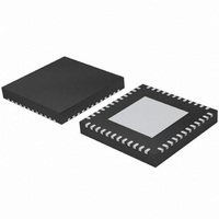
TDA9898HN/V2,551 NXP Semiconductors, TDA9898HN/V2,551 Datasheet - Page 84

TDA9898HN/V2,551
Manufacturer Part Number
TDA9898HN/V2,551
Description
IC IF PROCESSOR MULTISTD 48HVQFN
Manufacturer
NXP Semiconductors
Datasheet
1.TDA9898HNV3518.pdf
(103 pages)
Specifications of TDA9898HN/V2,551
Function
IF Processor
Rf Type
ATV, DVB, FM
Package / Case
48-VFQFN Exposed Pad
Lead Free Status / RoHS Status
Lead free / RoHS Compliant
Other names
935283079551
TDA9898HN/V2-S
TDA9898HN/V2-S
TDA9898HN/V2-S
TDA9898HN/V2-S
NXP Semiconductors
Table 56.
V
V
gain controlled amplifier adjusted to typical specified output level; measurements taken in test circuit of
crystal oscillator reference; unless otherwise specified.
[1]
[2]
[3]
[4]
[5]
[6]
[7]
[8]
[9]
Table 57.
[1]
[2]
TDA9897_TDA9898_4
Product data sheet
Symbol
R
I
f
22 to 29.5
30 to 37.5
38 to 45.5
46 to 53.5
57
swoff
VCO
P
i(IF)
swoff(FREF)
= 5 V
Some parameters can be decreased at V
This parameter is not tested during production and is only given as application information.
Output current can be increased by application of single-ended resistor from each output pin to GND. Recommended resistor value is
minimum 1 k .
With single-ended load for f
ground.
Noise level is measured without input signal but AGC adjusted corresponding to the given input level.
Set with AGC nominal output voltage as reference. For C/N measurement switch input signal off.
With single-ended load R
The tolerance of the reference frequency determines the accuracy of VIF AFC, RIF AFC, FM demodulator center frequency, maximum
FM deviation, sound trap frequency, LIF band-pass cut-off frequency, as well as the accuracy of the synthesizer.
The value of C
Calculation of the PLL loop filter by using the following formulae:
with the following parameters:
K
N = divider ratio:
K
R
C
B
d = damping factor.
If more than one frequency range is used in the application, then the smallest resistor value should be applied.
B
d
= 10 mV (RMS); f
(MHz)
O
D
LF( 3dB)
LFSYN2
LFSYN2
LF
=
= VCO steepness (Hz/V),
= phase detector steepness (A/rad),
[1]
–
1
-- - R
2
3dB
; T
Characteristics
Conversion synthesizer PLL; loop filter dimensions
= synthesizer loop filter serial resistor ( ),
= synthesizer loop filter serial capacitor (F),
LFSYN2
= 3 dB LF bandwidth (Hz),
amb
=
= 25 C; 8 MHz system; see
pull
K
------ -K
Parameter
switch-off resistance
on pin FREF
switch-off current
N
O
2
N
determines the accuracy of the resonance frequency of the crystal. It depends on the used type of crystal.
D
IF
K
------ -K
=
N
R
O
= 36 MHz for low IF output of 5 MHz; IF input from 50
------------------- -
0.5 MHz
LFSYN2
f
L
D
VCO
C
…continued
IF
1 k and C
LFSYN2
< 45 MHz R
, valid for d
,
L
P
L
Conditions
to switch off reference signal
input by external resistor
wired between pin FREF
and GND
R
R
R
1.5
1.8
2.2
2.7
3.3
= 4.5 V.
5 pF to ground.
swoff(FREF)
swoff(FREF)
LFSYN2
1.2
1 k and C
Table 33
(k )
Rev. 04 — 25 May 2009
= 3.9 k
= 22 k
L
and
[2]
5 pF to ground and for f
Table
34; CW test input signal is used for specification;
[1]
TDA9897; TDA9898
IF
Min
3.9
-
-
= 45 MHz to 60 MHz R
via broadband transformer 1 : 1;
Multistandard hybrid IF processing
C
4.7
4.7
4.7
4.7
4.7
LFSYN2
Typ
-
-
25
(nF)
L
= 1 k and C
Figure 51
Max
27
100
-
© NXP B.V. 2009. All rights reserved.
with 4 MHz
L
Unit
k
84 of 103
A
A
3 pF to


