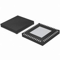
TDA9898HN/V2,551 NXP Semiconductors, TDA9898HN/V2,551 Datasheet - Page 63

TDA9898HN/V2,551
Manufacturer Part Number
TDA9898HN/V2,551
Description
IC IF PROCESSOR MULTISTD 48HVQFN
Manufacturer
NXP Semiconductors
Datasheet
1.TDA9898HNV3518.pdf
(103 pages)
Specifications of TDA9898HN/V2,551
Function
IF Processor
Rf Type
ATV, DVB, FM
Package / Case
48-VFQFN Exposed Pad
Lead Free Status / RoHS Status
Lead free / RoHS Compliant
Other names
935283079551
TDA9898HN/V2-S
TDA9898HN/V2-S
TDA9898HN/V2-S
TDA9898HN/V2-S
NXP Semiconductors
[5]
[6]
[7]
[8]
[9]
[10] Modulation VSB; sound carrier off; f
[11] Sound carrier on; f
[12] The sound carrier trap can be bypassed by setting the I
[13] Measurement condition: with transformer, transmitter pre-correction on; reference is at 1 MHz.
[14] The response time is valid for a VIF input level range from 200 V to 70 mV.
[15] AGC response time increased if no AGC event occurs during two lines at minimum.
[16] AGC response time increased if video level falls below half of selected level.
[17] Load applied to output pin causes signal loss. The resulting gain can be calculated by using
[18] See
[19] To match the AFC output signal to different tuning systems a current output is provided. The test circuit is given in
[20] The AFC value of the VIF and RIF frequency is generated by using digital counting methods. The used counter resolution is provided
[21] Measured with an FM deviation of 25 kHz and the typical AF output voltage of 500 mV (RMS). The audio signal processing stage
[22] Amplitude response depends on dimensioning of FM PLL loop filter.
[23] The lower AF cut-off frequency depends on the value of the capacitor at pin CAF. A value of C
[24] For all signal-to-noise measurements the used VIF modulator has to meet the following specifications:
[25] The PC / SC ratio is calculated as the addition of TV transmitter PC / SC1 ratio and SAW filter PC / SC1 ratio. This PC / SC ratio is
[26] Measurement condition is SC1 / SC2
[27] The differential QSS signal output on pins OUT1A and OUT1B is analyzed by a test demodulator TDA9820. The signal-to-noise ratio of
TDA9897_TDA9898_4
Product data sheet
B
using the following formulae:
with the following parameters:
K
K
R = loop filter serial resistor ( ),
C = loop filter serial capacitor (F),
B
d = damping factor.
The VCO frequency offset related to the PC frequency is set to 1 MHz with white picture video modulation.
AC load; C
carrier traps.
Condition: luminance range (5 steps) from 0 % to 100 %. Measurement value is based on 4 of 5 steps.
Measurement using 200 kHz high-pass filter, 5 MHz low-pass filter and subcarrier notch filter ( “ITU-T J.64” ).
spectrum appears at pin CVBS. The video amplitude is reduced to 1.1 V (p-p).
AFC steepness can be changed by different applications of resistors R1 and R2.
with an uncertainty of 1 bit corresponding to 25 kHz. This uncertainty of 25 kHz has to be added to the frequency accuracy
parameter.
provides headroom of 6 dB with THD < 1.5 %. The I
0 dB to 18 dB in steps of 6 dB. Reducing the audio gain for handling a frequency deviation of more than 55 kHz avoids AF output
signal clipping.
and C
a) Incidental phase modulation for black-to-white jump less than 0.5 degrees.
b) QSS AF performance, measured with the television demodulator AMF2 (audio output, weighted signal-to-noise ratio) better than
c) Picture-to-sound carrier ratio PC / SC1 = 13 dB (transmitter).
necessary to achieve the weighted signal-to-noise values as noted. A different PC / SC ratio will change these values.
this device is better than 60 dB. The measurement is related to an FM deviation of 27 kHz and in accordance with “ITU-R BS.468-4” .
B
d
LF( 3dB)
O
D
LF( 3dB)
LF
=
= VCO steepness (Hz/V),
= phase detector steepness (A/rad),
60 dB (at deviation 27 kHz) for 6 kHz sine wave black-to-white video modulation.
Figure 19
–
1
-- - R 2 K
2
AF1
3dB
= 100 kHz (damping factor d = 1.7; calculated with sync level within gain control range). Calculation of the VIF PLL filter by
= 3 dB LF bandwidth (Hz),
= 220 nF leads to f
L
=
< 20 pF and R
K
to smooth current pulses.
O
O
K
K
video
D
D
C
R
= 10 kHz to 10 MHz.
, valid for d
L
> 1 k . The sound carrier frequencies (depending on TV standard) are attenuated by the integrated sound
3dB(AF)l
video
1.2
40 Hz.
7 dB.
> 0.5 MHz.
2
Rev. 04 — 25 May 2009
C-bus bits W3[0] and W3[1] control the AF output signal amplitude from
2
C-bus bit W2[0] to logic 0; see
TDA9897; TDA9898
Table
Multistandard hybrid IF processing
G
23. In this way the full composite video
AF1
v(load)
= 470 nF leads to f
=
G
v
+
20
© NXP B.V. 2009. All rights reserved.
log
Figure
------------------- -
R
3dB(AF)l
O
R
+
19. The
L
R
L
63 of 103
20 Hz
.


