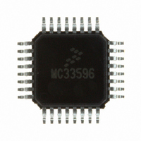
MC33596FJER2 Freescale Semiconductor, MC33596FJER2 Datasheet - Page 11

MC33596FJER2
Manufacturer Part Number
MC33596FJER2
Description
IC RX UHF PLL TUNED 32-LQFP
Manufacturer
Freescale Semiconductor
Datasheet
1.MC33596FCAE.pdf
(70 pages)
Specifications of MC33596FJER2
Frequency
304, 315, 426, 434, 868 & 915MHz
Sensitivity
-104dBm
Data Rate - Maximum
22.4 kBaud
Modulation Or Protocol
FSK, OOK
Applications
General Data Transfer
Current - Receiving
10.3mA
Data Interface
PCB, Surface Mount
Antenna Connector
PCB, Surface Mount
Voltage - Supply
2.7 V ~ 3.6 V, 4.5 V ~ 5.5 V
Operating Temperature
-40°C ~ 85°C
Package / Case
32-LQFP
Operating Temperature (min)
-40C
Operating Temperature (max)
85C
Operating Temperature Classification
Industrial
Modulation Type
FSK/OOK
Package Type
LQFP
Operating Supply Voltage (min)
2.7V
Lead Free Status / RoHS Status
Lead free / RoHS Compliant
Features
-
Memory Size
-
Lead Free Status / Rohs Status
Compliant
Available stocks
Company
Part Number
Manufacturer
Quantity
Price
Part Number:
MC33596FJER2
Manufacturer:
FREESCALE
Quantity:
20 000
Freescale Semiconductor
Refer to Table 5 for pins direction
Refer to Table 5 for pins direction
See
See
See
See
SPI Deselected
SPI Deselected
SPI Deselected
SPI Deselected
SPI Slave
SPI Slave
SPI Slave
SPI Slave
SPI Master
SPI Master
SPI Master
SPI Master
… and SOE = 1
… and SOE = 1
… and SOE = 1
… and SOE = 1
Figure3
Figure3
Figure3
Figure3
… and DME = 0
… and DME = 0
… and DME = 0
… and DME = 0
Activate Bank Change,
Activate Bank Change,
(A to B or B to A)
(A to B or B to A)
Power-on Reset
Power-on Reset
Power-on Reset
Power-on Reset
See
See
See
See
… and SOE = 0
… and SOE = 0
… and SOE = 0
… and SOE = 0
Figure 2. State Machine Overview
Figure4
Figure4
Figure4
Figure4
MC33596 Data Sheet, Rev. 4
State 1
State 1
State 60
State 60
Standby/LVD Mode
Standby/LVD Mode
Standby/LVD Mode
Standby/LVD Mode
Configuration Mode
Configuration Mode
Configuration Mode
Configuration Mode
CONFB = 0,
CONFB = 0,
CONFB = 0,
CONFB = 0,
and STROBE = 1
and STROBE = 1
and STROBE = 1
and STROBE = 1
CONFB = 1,
CONFB = 1,
CONFB = 1,
CONFB = 1,
TRXE = 1
TRXE = 1
TRXE = 1
TRXE = 1
See
See
See
See
… and SOE = 1
… and SOE = 1
… and SOE = 1
… and SOE = 1
Figure11
Figure11
Figure11
Figure11
CONFB = 1,
CONFB = 1,
CONFB = 1,
CONFB = 1,
TRXE = 1
TRXE = 1
TRXE = 1
TRXE = 1
CONFB = 1,
CONFB = 1,
CONFB = 1,
CONFB = 1,
and STROBE = 0
and STROBE = 0
and STROBE = 0
and STROBE = 0
CONFB = 0,
CONFB = 0,
CONFB = 0,
CONFB = 0,
and STROBE = 1
and STROBE = 1
and STROBE = 1
and STROBE = 1
… and DME = 1
… and DME = 1
… and DME = 1
… and DME = 1
State 30
State 30
See
See
See
See
Transmit Mode
Transmit Mode
Transmit Mode
Transmit Mode
… and SOE = 0
… and SOE = 0
… and SOE = 0
… and SOE = 0
Figure12
Figure12
Figure12
Figure12
State Machine
Receive Mode
Receive Mode
Receive Mode
Receive Mode
11


