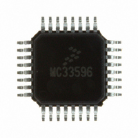
MC33596FJER2 Freescale Semiconductor, MC33596FJER2 Datasheet - Page 22

MC33596FJER2
Manufacturer Part Number
MC33596FJER2
Description
IC RX UHF PLL TUNED 32-LQFP
Manufacturer
Freescale Semiconductor
Datasheet
1.MC33596FCAE.pdf
(70 pages)
Specifications of MC33596FJER2
Frequency
304, 315, 426, 434, 868 & 915MHz
Sensitivity
-104dBm
Data Rate - Maximum
22.4 kBaud
Modulation Or Protocol
FSK, OOK
Applications
General Data Transfer
Current - Receiving
10.3mA
Data Interface
PCB, Surface Mount
Antenna Connector
PCB, Surface Mount
Voltage - Supply
2.7 V ~ 3.6 V, 4.5 V ~ 5.5 V
Operating Temperature
-40°C ~ 85°C
Package / Case
32-LQFP
Operating Temperature (min)
-40C
Operating Temperature (max)
85C
Operating Temperature Classification
Industrial
Modulation Type
FSK/OOK
Package Type
LQFP
Operating Supply Voltage (min)
2.7V
Lead Free Status / RoHS Status
Lead free / RoHS Compliant
Features
-
Memory Size
-
Lead Free Status / Rohs Status
Compliant
Available stocks
Company
Part Number
Manufacturer
Quantity
Price
Part Number:
MC33596FJER2
Manufacturer:
FREESCALE
Quantity:
20 000
Receive Mode
Each time is defined with the associated value found in the RXONOFF register.
The strobe oscillator is a relaxation oscillator in which an external capacitor C13 is charged by an internal
current source (see
The strobe frequency is F
In receive mode, setting the STROBE pin to V
the oscillator threshold voltage, the condition on which the STROBE pin is set to V
internally, and the oscillator pulldown circuitry is disabled. This limits the current consumption. After the
STROBE pin is forced to high level, the external driver should pass via a “0” state to discharge the
capacitor before going to high impedance state (otherwise, the on time would last a long time after the
driver release).
When the strobe oscillator is running (i.e., during an off time), forcing the STROBE pin to V
strobe clock, and therefore keeps the circuit off.
Figure 14
11.4 Received Signal Strength Indicator (RSSI)
11.4.1 Module Description
In receive mode, a received signal strength indicator can be activated by setting bit RSSIE.
The input signal is measured at two different points in the receiver chain by two different means, as
follows.
22
•
•
•
STROBE
STROBE
On time = RON[3:0] × 512 × T
Off time = receiver off time = N × T
from ROFF[2:0] (see
Receiver
At the IF filter output, a progressive compression logarithmic amplifier measures the input signal,
ranging from the sensitivity level up to –50 dBm.
Counter
Counter
Status
Digital
Clock
Clock
shows the associated timings.
Off
On
Threshold
0
RON
Figure
Strobe
46). When the threshold is reached, C13 is discharged and the cycle restarts.
Off
Table
Cycling Period
0
t
Strobe
= 1/T
ROFF-1 ROFF
Figure 14. Receiver On/Off Sequence
17)
Strobe
digclk
MC33596 Data Sheet, Rev. 4
with T
Strobe
(see
On
CCIO
Crystal Oscillator Startup
0
Table
Strobe
+ MIN (T
RON
at any time forces the circuit on. As V
= 10
16; begins after the crystal oscillator has started)
Off
Strobe
6
0
× C13.
/ 2, receiver on time), with N decoded
SET TO V
STROBE
RON
On
CCIO
CCIO
Freescale Semiconductor
is detected
CCIO
GND
is above
stops the


