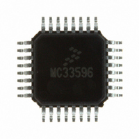
MC33596FJER2 Freescale Semiconductor, MC33596FJER2 Datasheet - Page 35

MC33596FJER2
Manufacturer Part Number
MC33596FJER2
Description
IC RX UHF PLL TUNED 32-LQFP
Manufacturer
Freescale Semiconductor
Datasheet
1.MC33596FCAE.pdf
(70 pages)
Specifications of MC33596FJER2
Frequency
304, 315, 426, 434, 868 & 915MHz
Sensitivity
-104dBm
Data Rate - Maximum
22.4 kBaud
Modulation Or Protocol
FSK, OOK
Applications
General Data Transfer
Current - Receiving
10.3mA
Data Interface
PCB, Surface Mount
Antenna Connector
PCB, Surface Mount
Voltage - Supply
2.7 V ~ 3.6 V, 4.5 V ~ 5.5 V
Operating Temperature
-40°C ~ 85°C
Package / Case
32-LQFP
Operating Temperature (min)
-40C
Operating Temperature (max)
85C
Operating Temperature Classification
Industrial
Modulation Type
FSK/OOK
Package Type
LQFP
Operating Supply Voltage (min)
2.7V
Lead Free Status / RoHS Status
Lead free / RoHS Compliant
Features
-
Memory Size
-
Lead Free Status / Rohs Status
Compliant
Available stocks
Company
Part Number
Manufacturer
Quantity
Price
Part Number:
MC33596FJER2
Manufacturer:
FREESCALE
Quantity:
20 000
LVDE (Low Voltage Detection Enable) enables the low voltage detection function.
CLKE (Clock Enable) controls the DATACLK output buffer.
Figure 25
DSREF (Data Slicer Reference) selects the data slicer reference.
In the case of FSK modulation (MODU = 1), DSREF must be set.
FRM (Frequency Register Manager) enables either a user friendly access or a direct access to one
frequency register.
MODU (Modulation) sets the data modulation type.
DR[1:0] (Data Rate) configure the receiver blocks operating in base band.
Freescale Semiconductor
Reset Value
Bit Name
Access
•
0 = disabled
1 = enabled
0 = DATACLK remains low
1 = DATACLK outputs F
0 = Fixed reference (cannot be used in FSK)
1 = Adaptive reference (recommended for maximum sensitivity in OOK and FSK)
0 = The carrier frequency is defined by the F register
1 = The local oscillator frequency is defined by the F register.
0 = On/Off Keying (OOK) modulation
1 = Frequency Shift Keying (FSK) modulation
Low-pass data filter
describes configuration register 2, CONFIG2.
This bit is cleared by POR. In the event of a complete loss of the supply
voltage, LVD is disabled at power-up, but the information is not lost as the
status bit LVDS is set by POR.
DSREF
Bit 7
R/W
0
FRM
Bit 6
R/W
0
SL
0
1
Table 9. Active Level of SWITCH Output Pin
dataclk
MODU
Bit 5
R/W
Figure 25. CONFIG2 Register
Receiver Function
0
MC33596 Data Sheet, Rev. 4
Receiving
Receiving
—
—
Bit 4
DR1
R/W
NOTE
1
Bit 3
DR0
R/W
0
Level on SWITCH
High
High
Low
Low
TRXE
Bit 2
R/W
0
DME
Bit 1
R/W
0
Register Description
SOE
Bit 0
R/W
0
Addr
$01
35


