EM250-RTR Ember, EM250-RTR Datasheet - Page 97
EM250-RTR
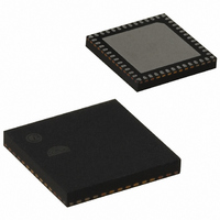
Manufacturer Part Number
EM250-RTR
Description
IC ZIGBEE SYSTEM-ON-CHIP 48-QFN
Manufacturer
Ember
Series
EM250r
Datasheet
1.EM250-JMP-R.pdf
(117 pages)
Specifications of EM250-RTR
Frequency
2.4GHz
Modulation Or Protocol
802.15.4 Zigbee
Applications
Home/Building Automation, Industrial Control and Monitoring
Power - Output
3dBm
Sensitivity
-97dBm
Voltage - Supply
2 V ~ 3.6 V
Current - Receiving
35.5mA
Current - Transmitting
33mA
Data Interface
PCB, Surface Mount
Memory Size
128kB Flash, 5kB SRAM
Antenna Connector
PCB, Surface Mount
Operating Temperature
-40°C ~ 85°C
Package / Case
48-QFN
For Use With
636-1009 - PROGRAMMER USB FLASH EM250/260
Lead Free Status / RoHS Status
Lead free / RoHS Compliant
Data Rate - Maximum
-
Other names
636-1000-2
Available stocks
Company
Part Number
Manufacturer
Quantity
Price
Company:

Part Number:
EM250-RTR
Manufacturer:
TI
Quantity:
3 400
Part Number:
EM250-RTR
Manufacturer:
EMBER
Quantity:
20 000


5.5
ADC Module
The ADC is a first-order sigma-delta converter sampling at 1MHz with programmable resolution and conversion
rate. The conversion rate is programmed by setting the
ADC_RATE[2:0]
0
1
2
3
4
5
6
7
The analog input of the ADC can be chosen from various sources and is configured with the
the
ADC0, ADC1, ADC2, or ADC3) or differential (routed to pairs ADC0-ADC1 and ADC2-ADC3). For selecting alter-
nate pin functions, refer to Table 17 and Table 18.
ADC_SEL[3:0]
0
1
2
3
4
5
6
7
8
9
10
Setting the
will continually generate conversions until the
INT_ADC
enabled in the
completes. After each
the next conversion.
To ensure the pipelined digital filter in the ADC is flushed,
to
The ADC uses an internal reference, VREF, which may be routed out to the alternate pin function of GPIO8,
VREF_OUT. VREF_OUT is only enabled when the
ADC_SEL
ADC_CFG
interrupt is generated. In order for this to interrupt the CPU the interrupt mask
ADC_EN
or
register. As described in Table 34, the ADC inputs can be single-ended (routed individually to
ADC_RATE
INT_CFG
Analog Source of ADC
ADC0
ADC1
ADC2
ADC3
(1/4) * VDD_PADS (2.1–3.6V pad supply)
(1/2) * VDD (1.8V core supply)
RESERVED
VSS (0V)
VREF
ADC0–ADC1
ADC2–ADC3
bit in the
INT_ADC
Conversion Time
32 µs
64 µs
128 µs
256 µs
512 µs
1024 µs
2048 µs
4096 µs
register. The
. Discard the first sample after
ADC_CFG
interrupt, the
INT_ADC
Table 33. ADC Conversion Rate
register will cause the ADC to immediately begin conversions. The ADC
Table 34. ADC Inputs
INT_ADC
ADC_EN
interrupt is the only means for determining when a conversion
ADC_EN
Equivalent ADC Bits
5, located in ADC_DATA[15:11]
6, located in ADC_DATA[15:10]
7, located in ADC_DATA[15:9]
8, located in ADC_DATA[15:8]
9, located in ADC_DATA[15:7]
10, located in ADC_DATA[15:6]
11, located in ADC_DATA[15:5]
12, located in ADC_DATA[15:4]
bit is cleared. When each conversion completes, an
ADC_RATE
interrupt bit must be cleared to detect completion of
ADC_EN
bit in the
ADC_EN
GPIO Pin
4
5
6
7
8
4–5
6–7
is set.
ADC_CFG
bits in the
should be cleared before changes are made
register is set. VREF is trimmed as
ADC_CFG
Purpose
Single-ended
Single-ended
Single-ended
Single-ended
Supply monitoring
Supply monitoring
Calibration
Calibration
Differential
Differential
register.
120-0082-000I
INT_ADC
ADC_SEL
EM250
must be
bits in
97
Related parts for EM250-RTR
Image
Part Number
Description
Manufacturer
Datasheet
Request
R

Part Number:
Description:
EM250 RCM BOARD
Manufacturer:
Ember
Datasheet:

Part Number:
Description:
EM250 BREAKOUT BOARD
Manufacturer:
Ember
Datasheet:

Part Number:
Description:
KIT JUMP START FOR EM250
Manufacturer:
Ember
Datasheet:

Part Number:
Description:
KIT EVAL EM250 RF TEST
Manufacturer:
Ember
Datasheet:

Part Number:
Description:
KIT DEV FOR EM250
Manufacturer:
Ember
Datasheet:

Part Number:
Description:
KIT DEV EMBER ZIGBEE W/PCWH
Manufacturer:
Custom Computer Services Inc (CCS)

Part Number:
Description:
PROGRAMMER USB FLASH EM250/260
Manufacturer:
Ember
Datasheet:

Part Number:
Description:
IC ZIGBEE SYSTEM-ON-CHIP 40-QFN
Manufacturer:
Ember
Datasheet:

Part Number:
Description:
IC RF TXRX ZIGBEE 128KB 48QFN
Manufacturer:
Ember
Datasheet:
Part Number:
Description:
IC RF TXRX ZIGBEE 192KB 48QFN
Manufacturer:
Ember
Datasheet:

Part Number:
Description:
INSIGHT ADAPTER FOR EM2XX
Manufacturer:
Ember
Datasheet:
Part Number:
Description:
PROGRAMMER USB FLASH EM250/260
Manufacturer:
Ember
Datasheet:
Part Number:
Description:
IC ZIGBEE SYSTEM-ON-CHIP 40-QFN
Manufacturer:
Ember
Datasheet:
Part Number:
Description:
IC RF TXRX ZIGBEE 128KB 48QFN
Manufacturer:
Ember
Datasheet:
Part Number:
Description:
IC RF TXRX ZIGBEE 192KB 48QFN
Manufacturer:
Ember
Datasheet: