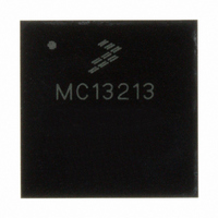
MC13213 Freescale Semiconductor, MC13213 Datasheet - Page 67

MC13213
Manufacturer Part Number
MC13213
Description
IC TXRX RF 2.4GHZ FLSH 60K 71LGA
Manufacturer
Freescale Semiconductor
Series
MC1321xr
Datasheet
1.1321XCSK-BDM.pdf
(70 pages)
Specifications of MC13213
Frequency
2.4GHz
Data Rate - Maximum
250kbps
Modulation Or Protocol
802.15.4 Zigbee
Applications
General Purpose
Power - Output
3dBm
Sensitivity
-92dBm
Voltage - Supply
1.8 V ~ 3.6 V
Current - Receiving
42mA
Current - Transmitting
35mA
Data Interface
PCB, Surface Mount
Memory Size
60kB Flash, 4kB RAM
Antenna Connector
PCB, Surface Mount
Operating Temperature
-40°C ~ 85°C
Package / Case
71-LGA
Number Of Receivers
1
Number Of Transmitters
1
Wireless Frequency
2.4 GHz to 2.48 GHz
Interface Type
SPI
Output Power
0 dBm to 2 dBm
Operating Supply Voltage
2 V to 3.4 V
Maximum Operating Temperature
+ 85 C
Mounting Style
SMD/SMT
Maximum Supply Current
42 mA
Minimum Operating Temperature
- 40 C
Protocol Supported
802.15.4
Lead Free Status / RoHS Status
Lead free / RoHS Compliant
Available stocks
Company
Part Number
Manufacturer
Quantity
Price
Company:
Part Number:
MC13213
Manufacturer:
FREESCALE Semiconductor
Quantity:
337
Part Number:
MC13213
Manufacturer:
FREESCALE
Quantity:
20 000
Company:
Part Number:
MC13213R2
Manufacturer:
BROADCOM
Quantity:
1
Part Number:
MC13213R2
Manufacturer:
FREESCALE
Quantity:
20 000
7.4
Figure 36
the RFIN and PAO ports are used and the internal T/R switch is bypassed. Matching is provided for both
differential ports by L5, L6, L7, and L9 and C4 and C7. A balun is used for both receive and transmit paths
which are provided by the external T/R switch, IC1. This implementation, while more complicated, gives
better performance due to the reduced loss of the external T/R switch and the more optimum match
provided to the PAO and RFIN ports.
The switch control is connected to the CT_Bias pin which serves as its control signal. The CT_Bias signal
can be programmed to be active high or active low (depending on TX versus RX) and will switch
appropriately based on the radio operation. No interaction with the MCU on an operation-by-operation
basis is required.
The VDD voltage to the antenna switch is connected to GPIO1. This is a useful feature when GPIO1 is
programmed as an “Out of Idle” status indicator. When the radio is out of Idle (or active), the antenna
switch is powered. In this manner, the antenna switch only consumes current when it needs to be active.
The GPIO1 can only be used as a VDD source for a very low current load.
Freescale Semiconductor
U2
MC1321x
RFIN_M
CT_Bias
RFIN_P
PAO_M
PAO_P
GPIO1
44
39
38
36
35
34
RF Dual Port Application with an F-Antenna
shows a typical dual port application topology which also uses a printed copper F antenna. Both
Passive component values can vary as a function of circuit board layout as
required to obtain best matching and RF performance.
Figure 36. RF Dual Port Application with an F-Antenna
L5
4.7nH
L6
4.7nH
L7
3.3nH
L9
3.3nH
MC13211/212/213 Technical Data, Rev. 1.8
C4
1.0pF
C7
1.8pF
VDDA
C6
10pF
3
2
4
3
2
4
Z2
LDB212G4005C-001
Z3
LDB212G4005C-001
NOTE
1
5
6
1
5
6
C3
10pF
C8
10pF
3
1
2
IC1
µPG2012TK-E2
OUT2
OUT1
GND
VCONT
VDD
IN
6
5
4
C5
10pF
L8
2.2nH
C9
1.8pF
2
3
4
5
R4
0R
Not Mounted
J2
SMA_edge_Receptacle_Female
R3
0R
ANT2
F_Antenna
67


