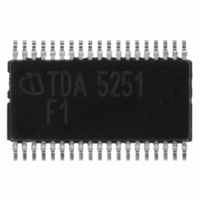
TDA5251 Infineon Technologies, TDA5251 Datasheet - Page 32

TDA5251
Manufacturer Part Number
TDA5251
Description
TXRX FSK/ASK SGL LP TSSOP-38
Manufacturer
Infineon Technologies
Type
Transceiverr
Specifications of TDA5251
Package / Case
38-TSSOP
Frequency
315MHz
Data Rate - Maximum
64kbps
Modulation Or Protocol
ASK, FSK
Applications
RKE, Remote Control Systems
Power - Output
13dBm
Sensitivity
-109dBm
Voltage - Supply
2.1 V ~ 5.5 V
Current - Receiving
9.3mA
Current - Transmitting
14mA
Data Interface
PCB, Surface Mount
Antenna Connector
PCB, Surface Mount
Operating Temperature
-40°C ~ 85°C
Operating Frequency
0.35 MHz
Operating Supply Voltage
2.5 V, 3.3 V, 5 V
Maximum Operating Temperature
+ 85 C
Minimum Operating Temperature
- 40 C
Mounting Style
SMD/SMT
Operating Temperature (min)
-40C
Operating Temperature (max)
85C
Operating Temperature Classification
Industrial
Product Depth (mm)
4.4mm
Product Length (mm)
9.7mm
Operating Supply Voltage (min)
2.1V
Operating Supply Voltage (max)
5.5V
Lead Free Status / RoHS Status
Lead free / RoHS Compliant
Memory Size
-
Lead Free Status / Rohs Status
Compliant
Other names
SP000014554
TDA5251
TDA5251INTR
TDA5251XT
TDA5251
TDA5251INTR
TDA5251XT
Available stocks
Company
Part Number
Manufacturer
Quantity
Price
Company:
Part Number:
TDA5251
Manufacturer:
INFINEON
Quantity:
276
Figure 2-13
D_OUT and RX_DATA_INV from the CONFIG register determine the output of data at Pin 28.
RxTxint and TX_ON are internally generated signals.
In RX and power down mode Data pin (Pin 28) is tied to GND.
Figure 2-14
2.4.18
The sequence timer has to control all the enable signals of the analog components inside the chip.
The time base is the 32 kHz RC oscillator.
After the first POWER ON or RESET a 730kHz clock is available at the clock output pin. This clock
output can be used by an external µP to set the system into the desired state and outputs valid data
after 500 µs (see Figure 2-15 and Figure 2-16, t CLKSU )
There are two possibilities to start the device after a reset or first power on:
−
−
Note: It is required to activate the device for the duration of t
Only if this is done the normal operation timing is performed.
Data Sheet
PWDDD pin is LOW: Normal operation timing is performed after t
PWDDD pin is HIGH (device in power down mode): A clock is offered at the clock output pin
until the device is activated (PWDDD pin is pulled to LOW). After the first activation the time
t
This could be used to extend the clock generation without device programming or activation.
SYSSU
is required until normal operation timing is performed (see Figure 2-16 ).
Sequence Timer
Data Valid Circuit
Data Input/Output Circuit
RX_DATA_INV
DATA VALID
RX DATA
TX DATA
RxTxint
D_OUT
TX ON
0,5*TH1
TH1
T
GATE
T
RSSI
GATE
0,5*TH2
TH2
TH3
32
SYSSU
DATA VALID
after first power on or a reset.
SYSSU
Data
28
Functional Description
(see Figure 2-15).
TDA5251 F1
Version 1.1
2007-02-26
data_switch.wmf
data_valid.wmf


