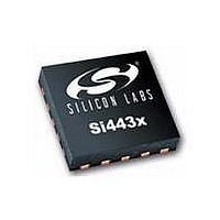
SI4431-B1-FM Silicon Laboratories Inc, SI4431-B1-FM Datasheet - Page 13

SI4431-B1-FM
Manufacturer Part Number
SI4431-B1-FM
Description
IC TXRX 240-930MHZ -8-13DB 20QFN
Manufacturer
Silicon Laboratories Inc
Specifications of SI4431-B1-FM
Package / Case
20-VQFN
Mfg Application Notes
Transitioning SI4430/31 to Rev B
Frequency
240MHz ~ 930MHz
Data Rate - Maximum
256kbps
Modulation Or Protocol
FSK, GFSK, OOK
Applications
General Purpose
Power - Output
13dBm
Sensitivity
-121dBm
Voltage - Supply
1.8 V ~ 3.6 V
Current - Receiving
18.5mA
Current - Transmitting
30mA
Data Interface
PCB, Surface Mount
Antenna Connector
PCB, Surface Mount
Operating Temperature
-40°C ~ 85°C
Wireless Frequency
240 MHz to 930 MHz
Output Power
13 dBm
Operating Supply Voltage
1.8 V to 3.6 V
Maximum Operating Temperature
+ 85 C
Mounting Style
SMD/SMT
Maximum Supply Current
30 mA
Minimum Operating Temperature
- 40 C
Modulation
FSK, GFSK, OOK
Operating Temperature (min)
-40C
Operating Temperature (max)
85C
Operating Temperature Classification
Industrial
Product Depth (mm)
4mm
Product Length (mm)
4mm
Operating Supply Voltage (min)
1.8V
Operating Supply Voltage (typ)
3V
Operating Supply Voltage (max)
3.6V
Lead Free Status / RoHS Status
Lead free / RoHS Compliant
Memory Size
-
Lead Free Status / Rohs Status
Lead free / RoHS Compliant
Available stocks
Company
Part Number
Manufacturer
Quantity
Price
Company:
Part Number:
SI4431-B1-FMR
Manufacturer:
TE
Quantity:
2 000
Part Number:
SI4431-B1-FMR
Manufacturer:
SILICON LABS/èٹ¯ç§‘
Quantity:
20 000
Table 8. Absolute Maximum Ratings
V
Instantaneous V
Sustained V
Voltage on Digital Control Inputs
Voltage on Analog Inputs
RX Input Power
Operating Ambient Temperature Range T
Thermal Impedance
Junction Temperature T
Storage Temperature Range T
Note: Stresses beyond those listed under “Absolute Maximum Ratings” may cause permanent damage to the device. These
DD
to GND
are stress ratings only and functional operation of the device at or beyond these ratings in the operational sections of
the specifications is not implied. Exposure to absolute maximum rating conditions for extended periods may affect
device reliability. Power Amplifier may be damaged if switched on without proper load or termination connected. TX
matching network design will influence TX V
RF-peak
RF-peak
to GND on TX Output Pin
JA
to GND on TX Output Pin
J
STG
Parameter
A
RF-peak
Rev 1.1
on TX output pin. Caution: ESD sensitive device.
Si4430/31/32-B1
–0.3, V
–0.3, V
–55 to +125
–40 to +85
–0.3, +3.6
–0.3, +8.0
–0.3, +6.5
Value
+125
+10
30
DD
DD
+ 0.3
+ 0.3
C/W
Unit
dBm
C
C
C
V
V
V
V
V
13


