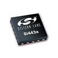
SI4431-B1-FM Silicon Laboratories Inc, SI4431-B1-FM Datasheet - Page 9

SI4431-B1-FM
Manufacturer Part Number
SI4431-B1-FM
Description
IC TXRX 240-930MHZ -8-13DB 20QFN
Manufacturer
Silicon Laboratories Inc
Specifications of SI4431-B1-FM
Package / Case
20-VQFN
Mfg Application Notes
Transitioning SI4430/31 to Rev B
Frequency
240MHz ~ 930MHz
Data Rate - Maximum
256kbps
Modulation Or Protocol
FSK, GFSK, OOK
Applications
General Purpose
Power - Output
13dBm
Sensitivity
-121dBm
Voltage - Supply
1.8 V ~ 3.6 V
Current - Receiving
18.5mA
Current - Transmitting
30mA
Data Interface
PCB, Surface Mount
Antenna Connector
PCB, Surface Mount
Operating Temperature
-40°C ~ 85°C
Wireless Frequency
240 MHz to 930 MHz
Output Power
13 dBm
Operating Supply Voltage
1.8 V to 3.6 V
Maximum Operating Temperature
+ 85 C
Mounting Style
SMD/SMT
Maximum Supply Current
30 mA
Minimum Operating Temperature
- 40 C
Modulation
FSK, GFSK, OOK
Operating Temperature (min)
-40C
Operating Temperature (max)
85C
Operating Temperature Classification
Industrial
Product Depth (mm)
4mm
Product Length (mm)
4mm
Operating Supply Voltage (min)
1.8V
Operating Supply Voltage (typ)
3V
Operating Supply Voltage (max)
3.6V
Lead Free Status / RoHS Status
Lead free / RoHS Compliant
Memory Size
-
Lead Free Status / Rohs Status
Lead free / RoHS Compliant
Available stocks
Company
Part Number
Manufacturer
Quantity
Price
Company:
Part Number:
SI4431-B1-FMR
Manufacturer:
TE
Quantity:
2 000
Part Number:
SI4431-B1-FMR
Manufacturer:
SILICON LABS/èٹ¯ç§‘
Quantity:
20 000
Table 3. Receiver AC Electrical Characteristics
RX Frequency
Range—Si4431/32
RX Frequency
Range—Si4430
RX Sensitivity
RX Channel Bandwidth
BER Variation vs Power
Level
LNA Input Impedance
(Unmatched—measured
differentially across RX
input pins)
RSSI Resolution
1-Ch Offset Selectivity
2-Ch Offset Selectivity
3-Ch Offset Selectivity
Blocking at 1 MHz Offset
Blocking at 4 MHz Offset
Blocking at 8 MHz Offset
Image Rejection
Spurious Emissions
Notes:
1. All specification guaranteed by production test unless otherwise noted. Production test conditions and max limits are listed
2. Receive sensitivity at multiples of 30 MHz may be degraded. If channels with a multiple of 30 MHz are required it is
3. Guaranteed by qualification. Qualification test conditions are listed in the "Production Test Conditions" section on page 14.
3
in the "Production Test Conditions" section on page 14.
recommended to shift the crystal frequency. Contact Silicon Labs Applications Support for recommendations.
Parameter
2
3
3
3
3
3
3
3
3
3
3
1M
4M
8M
P
RES
P
P
Symbol
P
P
P
C/I
C/I
C/I
R
P
RX_OOK
Im
RX_RES
OB_RX1
RX_100
RX_125
RX_40
F
F
BW
IN-RX
RX_2
BLOCK
BLOCK
BLOCK
1-CH
2-CH
3-CH
RX
RX
REJ
RSSI
lated with 40 kbps F = 20 kHz GFSK with
BER < 0.1%. Interferer and desired modu-
Desired Ref Signal 3 dB above sensitivity,
Desired Ref Signal 3 dB above sensitivity.
40 kbps F = 20 kHz GFSK with BT = 0.5
Interferer and desired modulated with
BT = 0.5, channel spacing = 150 kHz
Rejection at the image frequency.
(4.8 kbps, 350 kHz BW, OOK)
(40 kbps, 400 kHz BW, OOK)
(100 kbps, GFSK, BT = 0.5,
(125 kbps, GFSK, BT = 0.5,
(40 kbps, GFSK, BT = 0.5,
Up to +5 dBm Input Level
(2 kbps, GFSK, BT = 0.5,
Measured at RX pins
f = 62.5 kHz)
f = 20 kHz)
f = 50 kHz)
(BER < 0.1%)
(BER < 0.1%)
(BER < 0.1%)
(BER < 0.1%)
(BER < 0.1%)
(BER < 0.1%)
f = 5 kHz)
1
Rev 1.1
Conditions
IF=937 kHz
915 MHz
868 MHz
433 MHz
315 MHz
3
3
3
3
3
Si4430/31/32-B1
Min
240
900
2.6
—
—
—
—
—
—
—
—
—
—
—
—
—
—
—
—
—
—
—
—
107–137j
89–110j
51–60j
54–63j
–121
–108
–104
–101
–102
–110
±0.5
Typ
–31
–35
–40
–52
–56
–63
–30
—
—
—
—
0
Max
930
960
620
–54
0.1
—
—
—
—
—
—
—
—
—
—
—
—
—
—
—
—
—
—
Units
MHz
MHz
dBm
dBm
dBm
dBm
dBm
dBm
ppm
dBm
kHz
dB
dB
dB
dB
dB
dB
dB
dB
9


