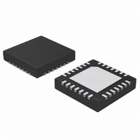
ATA5278-PKQI Atmel, ATA5278-PKQI Datasheet - Page 11

ATA5278-PKQI
Manufacturer Part Number
ATA5278-PKQI
Description
IC ANTENNA DVR STAND-ALONE 28QFN
Manufacturer
Atmel
Type
Stand Alone Antenna Driverr
Datasheet
1.ATA5278-PKQI.pdf
(34 pages)
Specifications of ATA5278-PKQI
Rf Type
TPM
Frequency
125kHz
Package / Case
28-VFQFN
Maximum Operating Temperature
+ 105 C
Mounting Style
SMD/SMT
Minimum Operating Temperature
- 40 C
Lead Free Status / RoHS Status
Lead free / RoHS Compliant
Features
-
Lead Free Status / Rohs Status
Lead free / RoHS Compliant
Other names
ATA5278-PKQITR
3.8
4832D–RKE–12/07
Command Description
Table 3-1 on page 10
ATA5278. Each command consists of one or more data words which the controller has to trans-
fer to the SPI of the ATA5278. An SPI data word is always eight bits in width and has to be
transferred starting with the least significant bit (LSB).
The following list contains detailed information on every command of the chip.
• The main purpose of command 1 is to check the operational status of the chip. Only if the
• Command 2 is the first out of three special function commands. It is used to reset the
• Command 3 can be used to stop the LF data transmission immediately. Regularly, the
• Command 4 has to be used to shut down the IC. In order to start the power-down sequence
• Command 5 is used to write configuration data into register 1, which is used for LF data
• Command 6 can be used to validate a change in register 1 (i.e., a prior command 5
• Command 7 writes configuration data to register 2, which handles timing relevant setup
• Command 8 can be used to validate a change of register 2 (i.e., a prior command 7
System-Ready bit (SR) and the Ready-To-Send bit (RTS) have been received as 1, the
ATA5278 is fully functional. In special cases, only the SR bit will be received as 1. This is
when the LF data buffer is full or when the power stages have been shut down due to a fault.
This command can be used at any time to check the status of the chip.
internal fault memory. Once a fault is detected by the internal diagnosis stage, it is stored in
the fault memory (i.e., the status register) and the power stages are shut down to protect
them from damage. In order to enable the chip again, this command has to be sent to the IC.
modulator stage works as long as new (i.e., unsent) LF data is in the data buffer. When using
this command, all data in the buffer will be deleted and the antenna driver stage is switched
to idle mode.
properly, no further command must be transmitted to the chip and the chip-select line (S_CS)
has to be disabled afterwards.
modulation control. All register access commands are of a 16-bit structure (i.e., two data
words). The first data word defines the access itself (i.e., read or write, and the register
number). The second data word is the configuration data, which is to be sent to the ATA5278.
Note that in return for the second data word, the first input data word is sent back to the
controller. This can be used to validate the SPI transmission. Register 1 contains the
four-bit-wide antenna coil current selector (IC3..IC0) and the modulation type selector bit
(NASK_PSK). For further details, please refer to the section
19.
operation) or to check its actual state after a power-down period. Like all register access
commands, it consists of two data words. The return data in the second data word has the
same bit sequence as in command 5.
information. Like all register access commands, it consists of two data words, where the
second one is the configuration data itself. Note that in return for the second data word, the
first input data word is sent back to the controller. This can be used to validate the SPI
transmission. Register 2 contains the two-bit-wide LF data baud-rate selector (BR1..BR0)
and the pin CLKO prescaler bit. For further details, please refer to the sections
Modulation” on page 13
operation) or to check its actual state after a power-down period. Like all register access
commands, it consists of two data words. The return data in the second data word has the
same bit sequence as in command 7.
summarizes the commands interpreted by the SPI control logic of the
and “Clock Supply”.
“Current Adjustment” on page
ATA5278
“LF Data
11


