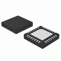
ATA5278-PKQI Atmel, ATA5278-PKQI Datasheet - Page 16

ATA5278-PKQI
Manufacturer Part Number
ATA5278-PKQI
Description
IC ANTENNA DVR STAND-ALONE 28QFN
Manufacturer
Atmel
Type
Stand Alone Antenna Driverr
Datasheet
1.ATA5278-PKQI.pdf
(34 pages)
Specifications of ATA5278-PKQI
Rf Type
TPM
Frequency
125kHz
Package / Case
28-VFQFN
Maximum Operating Temperature
+ 105 C
Mounting Style
SMD/SMT
Minimum Operating Temperature
- 40 C
Lead Free Status / RoHS Status
Lead free / RoHS Compliant
Features
-
Lead Free Status / Rohs Status
Lead free / RoHS Compliant
Other names
ATA5278-PKQITR
3.12
16
Driver Stage
ATA5278
The gate of the external transistor is driven by the QSC pin of the ATA5278. The signal provided
here is suited to drive standard MOSFETs (i.e., no logic-level FETs). During power-down mode
or a fault shutdown, the external transistor is switched off. Otherwise, this would lead to a con-
ducting state as long as no data modulation takes place. For further information on this pin,
please refer to the table “Electrical Characteristics” on
The driver stage of the ATA5278 consists of following blocks:
All these blocks are controlled by the internal driver control logic. The antenna driver stage itself
is supplied by the boost converter output voltage, which is applied at the VDS pin. It consists of
two power NMOS transistors in half-bridge configuration. As the high-side transistor requires a
control voltage above the output voltage (i.e., a voltage above the supply voltage VDS), a boot-
strap configuration is implemented. This circuitry requires an external capacitor of 10 nF to
22 nF, connected between the driver output and the CBOOST pin. This capacitor is charged
during the time when the low-side transistor is active. As soon as the low-side transistor is
switched off and the high-side transistor starts conducting, both the voltage at the DRV1 pin and
the CBOOST pin rises, but always with CBOOST being higher than DRV1 and hence being able
to provide an appropriate control voltage for the transistor.
ping configuration.
Figure 3-12. Bootstrap Configuration Circuitry
The output signal of the antenna driver stage is of a square wave shape. The duty cycle of this
signal is dependant on the selected antenna current. For further details, please refer to the sec-
tion
• DMOS half-bridge antenna driver
• Switched Mode Power Supply (SMPS) in boost configuration
• Antenna current sensor for peak value and zero-crossing detection
“Current Adjustment” on page
CBOOST
AGND
DRV1
VDS
19.
HS transistor
LS transistor
page
Figure 3-12
27.
Charge supply
High side driver
Low side driver
control signal
control signal
voltage
illustrates this boot strap-
4832D–RKE–12/07


