CLC030VEC National Semiconductor, CLC030VEC Datasheet - Page 12
CLC030VEC
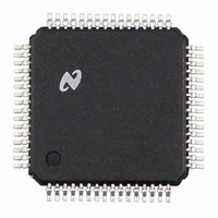
Manufacturer Part Number
CLC030VEC
Description
IC SERIALIZER VIDEO DGTL 64-TQFP
Manufacturer
National Semiconductor
Datasheet
1.CLC030VEC.pdf
(29 pages)
Specifications of CLC030VEC
Function
Serializer
Data Rate
1.485Gbps
Input Type
CMOS
Output Type
CMOS
Number Of Inputs
7
Number Of Outputs
7
Voltage - Supply
2.5V, 3.3V
Operating Temperature
0°C ~ 70°C
Mounting Type
Surface Mount
Package / Case
64-TQFP
Lead Free Status / RoHS Status
Contains lead / RoHS non-compliant
Other names
*CLC030VEC
Available stocks
Company
Part Number
Manufacturer
Quantity
Price
Company:

Part Number:
CLC030VEC
Manufacturer:
NSC
Quantity:
5 510
Company:
Part Number:
CLC030VEC
Manufacturer:
TI
Quantity:
5 510


www.national.com
Device Operation
Writing of ancillary data to the FIFO, packet handling and
insertion into the video data stream are controlled by a
MULTI-FUNCTION I/O PORT
The Multi-function I/O port can be configured to provide
immediate access to many control and indicator functions
within the CLC030 configuration and control registers. The
individual pins comprising this port may be assigned as input
or output for selected bits in the control data registers. The
multi-function I/O port is configured by way of an 8x6-bit
register bank, I/O pin 0 CONFIG through I/O pin 7 CONFIG.
The pin configuration registers contain codes which assign a
control register bit to a particular I/O pin. Controls and indi-
cators that are accessible by the port and their correspond-
ing selection addresses are given in the I/O Pin Configura-
tion Register Addresses, Table 6. Table 2 gives the control
register bit assignments.
Caution: When writing data into the control registers via the
multi-function I/O port, ACLK must be toggled to register the
data as shown in Figure 4. It is not necessary to toggle
ACLK when reading data from the multi-function I/O port.
Example: Program multi-function I/O port bit-0 as the CRC
Luma Error bit output.
1. Set ANC/CTRL to a logic-low.
2. Set RD/WR to a logic-low.
3. Present 00Fh to AD[9:0] as the I/O PIN 0 CONFIG
4. Toggle ACLK.
5. Present 310h to AD[9:0] as the register data.
6. Toggle ACLK.
register address.
FIGURE 4. I/O Port Data Write Timing
(Continued)
FIGURE 3. Ancillary Data Write Timing
20000312
12
system of masking and control bits in the control registers.
These and other ancillary data control functions such as
CHKSUM ATTACH IN are explained in detail later in this
data sheet.
EDH/CRC SYSTEM
The CLC030 has EDH and CRC character generation and
insertion circuitry. The EDH system functions as described
in SMPTE Recommended Practice RP-165. The CRC sys-
tem functions as specified in SMPTE 292M. The EDH/CRC
polynomial generators accept parallel data from the input
register and generate the EDH and CRC check words for
insertion in the serial data. Incoming parallel data is checked
for errors and the EDH flags are updated automatically. EDH
check words and status flags for SDTV data are generated
using the polynomial X
EDH check words are inserted in the serial data stream at
the correct positions in the ancillary data space and format-
ted per SMPTE 291M. Generation and automatic insertion of
the EDH check words is controlled by EDH Force and EDH
Enable bits in the control registers. After a reset, the initial
state of all EDH and CRC check characters is 00h.
The SMPTE 292M high definition video standard employs
CRC (cyclic redundancy check codes) error checking in-
stead of EDH. The CRC consists of two 18-bit words gener-
ated using the polynomial X
292M. One CRC is used for luminance and one for chromi-
nance data. CRC data is inserted at the required place in the
video data according to SMPTE 292M. The CRCs appear in
the data stream following the EAV and line number charac-
ters.
EDH and CRC errors are reported in the EDH0, EDH1, and
EDH2 register sets of the configuration and control registers.
PHASE-LOCKED LOOP SYSTEM
The phase-locked loop (PLL) system generates the output
serial data clock at 10x (standard definition) or 20x (high
definition) the parallel data clock frequency. This system
consists of a VCO, dividers, phase-frequency detector and
internal loop filter. The VCO free-running frequency is inter-
nally set. The parallel data clock V
PLL. The PLL automatically generates the appropriate fre-
quency for the serial clock rate. Loop filtering is internal to
the CLC030. The VCO has separate analog and digital
power supply feeds: V
DPLLD
pin 1, and V
SSPLLD
16
DDPLLA
+ X
pin 2. These may be separately
12
18
pin 62, V
+ X
+ X
CLK
6
20000311
5
+ 1 per SMPTE RP165.
+ X
is the reference for the
SSPLLA
4
+ 1 per SMPTE
pin 61, V
D -
Related parts for CLC030VEC
Image
Part Number
Description
Manufacturer
Datasheet
Request
R

Part Number:
Description:
Smpte 292m/259m Digital Video Serializer With Video And Ancilliary Data Fifos And Integrated Cable Driver
Manufacturer:
National Semiconductor Corporation
Datasheet:

Part Number:
Description:
National Semiconductor [8-Bit D/A Converter]
Manufacturer:
National Semiconductor
Datasheet:
Part Number:
Description:
National Semiconductor [Media Coprocessor]
Manufacturer:
National Semiconductor
Datasheet:
Part Number:
Description:
Digitally Controlled Tone and Volume Circuit with Stereo Audio Power Amplifier, Microphone Preamp Stage and National 3D Sound
Manufacturer:
National Semiconductor
Datasheet:
Part Number:
Description:
Digitally Controlled Tone and Volume Circuit with Stereo Audio Power Amplifier, Microphone Preamp Stage and National 3D Sound
Manufacturer:
National Semiconductor
Datasheet:
Part Number:
Description:
AC97 Rev 2 Codec with Sample Rate Conversion and National 3D Sound
Manufacturer:
National Semiconductor
Part Number:
Description:
Manufacturer:
National Semiconductor
Datasheet:
Part Number:
Description:
Manufacturer:
National Semiconductor
Datasheet:
Part Number:
Description:
General Purpose, Low Voltage, Low Power, Rail-to-Rail Output Operational Amplifiers
Manufacturer:
National Semiconductor
Datasheet:
Part Number:
Description:
8-bit 20 MSPS flash A/D converter.
Manufacturer:
National Semiconductor
Datasheet:
Part Number:
Description:
Low Noise Quad Operational Amplifier
Manufacturer:
National Semiconductor
Datasheet:
Part Number:
Description:
Quad Differential Line Receivers
Manufacturer:
National Semiconductor
Datasheet:
Part Number:
Description:
Quad High Speed Trapezoidal? Bus Transceiver
Manufacturer:
National Semiconductor
Datasheet:
Part Number:
Description:
Dual Line Receiver
Manufacturer:
National Semiconductor
Datasheet: