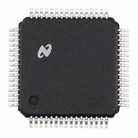
CLC030VEC National Semiconductor, CLC030VEC Datasheet - Page 6

CLC030VEC
Manufacturer Part Number
CLC030VEC
Description
IC SERIALIZER VIDEO DGTL 64-TQFP
Manufacturer
National Semiconductor
Datasheet
1.CLC030VEC.pdf
(29 pages)
Specifications of CLC030VEC
Function
Serializer
Data Rate
1.485Gbps
Input Type
CMOS
Output Type
CMOS
Number Of Inputs
7
Number Of Outputs
7
Voltage - Supply
2.5V, 3.3V
Operating Temperature
0°C ~ 70°C
Mounting Type
Surface Mount
Package / Case
64-TQFP
Lead Free Status / RoHS Status
Contains lead / RoHS non-compliant
Other names
*CLC030VEC
Available stocks
Company
Part Number
Manufacturer
Quantity
Price
Company:
Part Number:
CLC030VEC
Manufacturer:
NSC
Quantity:
5 510
Company:
Part Number:
CLC030VEC
Manufacturer:
TI
Quantity:
5 510
www.national.com
I
I
I
f
DC
f
DC
t
BR
t
t
t
t
t
t
t
t
t
t
DD
DD
DD
VCLK
ACLK
r
r
r
j
j
LOCK
LOCK
S
H
S
H
Symbol
Symbol
, t
, t
, t
DC Electrical Characteristics
Over Supply Voltage and Operating Temperature ranges, unless otherwise specified (Notes 2, 3).
AC Electrical Characteristics
Over Supply Voltage and Operating Temperature ranges, unless otherwise specified (Note 3).
Note 1: “Absolute Maximum Ratings” are those parameter values beyond which the life and operation of the device cannot be guaranteed. The stating herein of
these maximums shall not be construed to imply that the device can or should be operated at or beyond these values. The table of “Electrical Characteristics”
specifies acceptable device operating conditions.
Note 2: Current flow into device pins is defined as positive. Current flow out of device pins is defined as negative. All voltages are referenced to V
Note 3: Typical values are stated for V
Note 4: Spec. is guaranteed by design.
Note 5: R
Note 6: R
Note 7: Measured from rising-edge of first DV
V
A
f
SDO
f
f
(3.3V) Power Supply Current,
(2.5V) Power Supply Current,
(2.5V) Power Supply Current,
L
L
= 75Ω, AC-coupled
= 75Ω, AC-coupled
3.3V Supply, Total
2.5V Supply, Total
2.5V Supply, Total
Parallel Video Clock
Frequency
Video Clock Duty
Cycle
Ancillary Clock
Frequency
Ancillary Clock Duty
Cycle
Input Clock and Data
Rise Time, Fall Time
Serial Data Rate
Rise Time, Fall Time
Rise Time, Fall Time
Output Overshoot
Serial Output Jitter,
Intrinsic
Serial Output Jitter,
Intrinsic
Lock Time
Lock Time
Setup Time, Video
Data
Hold Time, Video Data
Setup Time, Anc. Data
Port
Hold Time, Anc. Data
Port
Parameter
Parameter
@
@
270 M
1,485 M
DDIO
bps
bps
, R
= V
10%–90%
(Notes 5, 6)
20%–80%, (Note 6)
20%–80%, (Note 5)
(Note 4)
270 M
1,485 M
(Notes 5, 7) (SD Rates)
(Notes 6, 7) (HD Rates)
Timing Diagram, (Note 4)
Timing Diagram, (Note 4)
Timing Diagram, (Note 4)
Timing Diagram, (Note 4)
, R
CLK
REF
DDSD
REF
V
color Bar Pattern, Test
Circuit, Test Loads Shall
Apply
V
color Bar Pattern, Test
Circuit, Test Loads Shall
Apply
V
color Bar Pattern, Test
Circuit, Test Loads Shall
Apply
LVL = R
CLK
CLK
CLK
cycle until Lock Detect output goes high (true). Lock time includes format detection time plus PLL lock time.
LVL = R
bps
= +3.3V, V
bps
= 74.25 MHz, NTSC
= 27 MHz, NTSC
= 74.25 MHz, NTSC
, (Notes 5, 9, 10)
REF
Conditions
, (Notes 6, 9, 10)
Conditions
REF
PRE = 4.75 kΩ 1%, See Test Loads and Test Circuit.
(Continued)
PRE = 4.75 kΩ 1%, See Test Loads and Test Circuit.
DDD
= V
DDPLL
= +2.5V and T
6
V
V
V
V
V
DDIO
DDD
DDPLL
DDD
DDPLL
Reference
V
V
A
A
V
AD
SDO, SDO
SDO, SDO
SDO, SDO
SDO, SDO
SDO, SDO
SDO, SDO
DV
V
AD
A
, V
, V
, V
A
CLK
CLK
CLK
CLK
CLK
CLK
CLK
= +25˚C.
DDZ
DDZ
N
N
N
Reference
DDSD
, A
to V
to A
to DV
to AD
,
,
CLK
CLK
CLK
, DV
N
N
Min
N
,
Min
270
1.0
27
45
45
Typ
66
66
85
Typ
500
200
120
1.5
1.5
1.5
1.5
1.5
50
50
15
15
5
Max
110
90
85
74.25
1,485
V
Max
270
3.0
2.0
2.0
2.0
2.0
55
55
CLK
SS
= 0V.
Units
Units
ps
ps
MHz
MHz
M
mA
mA
mA
ms
ms
ns
ps
ps
ns
ns
ns
ns
%
%
%
bps
P-P
P-P


