CLC030VEC National Semiconductor, CLC030VEC Datasheet - Page 5
CLC030VEC
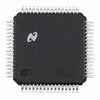
Manufacturer Part Number
CLC030VEC
Description
IC SERIALIZER VIDEO DGTL 64-TQFP
Manufacturer
National Semiconductor
Datasheet
1.CLC030VEC.pdf
(29 pages)
Specifications of CLC030VEC
Function
Serializer
Data Rate
1.485Gbps
Input Type
CMOS
Output Type
CMOS
Number Of Inputs
7
Number Of Outputs
7
Voltage - Supply
2.5V, 3.3V
Operating Temperature
0°C ~ 70°C
Mounting Type
Surface Mount
Package / Case
64-TQFP
Lead Free Status / RoHS Status
Contains lead / RoHS non-compliant
Other names
*CLC030VEC
Available stocks
Company
Part Number
Manufacturer
Quantity
Price
Company:

Part Number:
CLC030VEC
Manufacturer:
NSC
Quantity:
5 510
Company:
Part Number:
CLC030VEC
Manufacturer:
TI
Quantity:
5 510


V
V
V
V
V
V
V
T
t
V
V
I
I
V
V
V
I
JIT
IH
IL
DD
Symbol
Symbol
A
DDIO
DDSD
DDD
DDPLL
DDZ
IL
IH
IH
IL
OH
OL
SDO
Absolute Maximum Ratings
is anticipated that this device will not be offered in a
military qualified version. If Military/Aerospace specified
devices are required, please contact the National Semicon-
ductor Sales Office / Distributors for availability and specifi-
cations.
Recommended Operating Conditions
DC Electrical Characteristics
Over Supply Voltage and Operating Temperature ranges, unless otherwise specified (Notes 2, 3).
CMOS I/O Supply Voltage
SDO Supply Voltage
Digital Logic Supply Voltage
PLL Digital Supply Voltage
PLL Analog Supply Voltage
CMOS Input Voltage
(3.3V) Power Supply Current,
(V
(V
(V
(V
(V
(Vi):
DDIO
DDSD
DDD
DDPLL
DDPLLA
–V
–V
CMOS I/O Supply Voltage V
SDO Supply Voltage
Digital Logic Supply
Voltage
PLL Supply Voltage
Analog Supply Voltage
CMOS Input Voltage, Low
Level
CMOS Input Voltage High
Level
Operating Free Air
Temperature
Video Clock Jitter
Input Voltage High Level
Input Voltage Low Level
Input Current High Level
Input Current Low Level
CMOS Output Voltage
High Level
CMOS Output Voltage
Low Level
Serial Driver Output
Voltage
3.3V Supply, Total
–V
–V
SSD
–V
SSIO
SSSD
SSPLL
SSPLLA
):
):
):
Parameter
Parameter
):
), (V
DDZ
−V
SSD
) :
V
V
V
V
V
V
I
I
Test Circuit, Test Loads
Shall Apply
V
color Bar Pattern, Test
Circuit, Test Loads Shall
Apply
OH
OL
DDIO
DDSD
DDD
DDPLL
DDZ
IH
IL
CLK
= V
= +6.6 mA
= V
= −6.6 mA
–V
–V
= 27 MHz, NTSC
V
−V
−V
–V
SSIO
SSIO
DDIO
Conditions
SSD
Conditions
V
SSD
(Note 1) It
SSIO
SSSD
DDIO
SSPLL
−0.15V to
+0.15V
4.0V
4.0V
3.0V
3.0V
3.0V
5
CMOS Output Voltage
CMOS Input Current (single input):
CMOS Output Source/Sink Current:
SDO Output Sink Current:
Package Thermal Resistance
Storage Temp. Range:
Junction Temperature:
Lead Temperature (Soldering 4 Sec):
ESD Rating (HBM):
ESD Rating (MM):
V
All LVCMOS
Inputs
All LVCMOS
Outputs
SDO, SDO
V
CLK
DDIO
(Vo):
Vi = V
Vi = V
θ
θ
θ
JA
JA
JC
Reference
Reference
, V
@
@
SSIO
DDIO
0 LFM Airflow
500 LFM Airflow
DDSD
−0.15V:
+0.15V:
V
V
V
3.150 3.300
3.150 3.300
2.375 2.500
2.375 2.500
2.375 2.500
Min
Min
720
2.0
2.4
SSIO
SSIO
SSIO
0
V
+0.3
Typ
Typ
+90
800
2.7
SSIO
30
−1
48
V
V
V
+0.5V
3.450
3.450
2.625
2.625
2.625
V
+150
Max
Max
+70
−20
880
0.8
DDIO
DDIO
DDIO
SSIO
65
−65˚C to +150˚C
V
SSIO
V
www.national.com
DDIO
−0.15V to
±
6.5˚C/W
47˚C/W
27˚C/W
+150˚C
+260˚C
+0.15V
−5 mA
+5 mA
10 mA
40 mA
mV
Units
Units
ps
250V
mA
µA
µA
2 kV
˚C
V
V
V
V
V
V
V
V
V
V
V
P-P
P-P
Related parts for CLC030VEC
Image
Part Number
Description
Manufacturer
Datasheet
Request
R

Part Number:
Description:
Smpte 292m/259m Digital Video Serializer With Video And Ancilliary Data Fifos And Integrated Cable Driver
Manufacturer:
National Semiconductor Corporation
Datasheet:

Part Number:
Description:
National Semiconductor [8-Bit D/A Converter]
Manufacturer:
National Semiconductor
Datasheet:
Part Number:
Description:
National Semiconductor [Media Coprocessor]
Manufacturer:
National Semiconductor
Datasheet:
Part Number:
Description:
Digitally Controlled Tone and Volume Circuit with Stereo Audio Power Amplifier, Microphone Preamp Stage and National 3D Sound
Manufacturer:
National Semiconductor
Datasheet:
Part Number:
Description:
Digitally Controlled Tone and Volume Circuit with Stereo Audio Power Amplifier, Microphone Preamp Stage and National 3D Sound
Manufacturer:
National Semiconductor
Datasheet:
Part Number:
Description:
AC97 Rev 2 Codec with Sample Rate Conversion and National 3D Sound
Manufacturer:
National Semiconductor
Part Number:
Description:
Manufacturer:
National Semiconductor
Datasheet:
Part Number:
Description:
Manufacturer:
National Semiconductor
Datasheet:
Part Number:
Description:
General Purpose, Low Voltage, Low Power, Rail-to-Rail Output Operational Amplifiers
Manufacturer:
National Semiconductor
Datasheet:
Part Number:
Description:
8-bit 20 MSPS flash A/D converter.
Manufacturer:
National Semiconductor
Datasheet:
Part Number:
Description:
Low Noise Quad Operational Amplifier
Manufacturer:
National Semiconductor
Datasheet:
Part Number:
Description:
Quad Differential Line Receivers
Manufacturer:
National Semiconductor
Datasheet:
Part Number:
Description:
Quad High Speed Trapezoidal? Bus Transceiver
Manufacturer:
National Semiconductor
Datasheet:
Part Number:
Description:
Dual Line Receiver
Manufacturer:
National Semiconductor
Datasheet: