CLC030VEC National Semiconductor, CLC030VEC Datasheet - Page 21
CLC030VEC
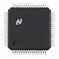
Manufacturer Part Number
CLC030VEC
Description
IC SERIALIZER VIDEO DGTL 64-TQFP
Manufacturer
National Semiconductor
Datasheet
1.CLC030VEC.pdf
(29 pages)
Specifications of CLC030VEC
Function
Serializer
Data Rate
1.485Gbps
Input Type
CMOS
Output Type
CMOS
Number Of Inputs
7
Number Of Outputs
7
Voltage - Supply
2.5V, 3.3V
Operating Temperature
0°C ~ 70°C
Mounting Type
Surface Mount
Package / Case
64-TQFP
Lead Free Status / RoHS Status
Contains lead / RoHS non-compliant
Other names
*CLC030VEC
Available stocks
Company
Part Number
Manufacturer
Quantity
Price
Company:

Part Number:
CLC030VEC
Manufacturer:
NSC
Quantity:
5 510
Company:
Part Number:
CLC030VEC
Manufacturer:
TI
Quantity:
5 510


Device Operation
control register instead of the multi-function I/O port, bit 7,
the I/O port bit must be remapped to another bit in the control
registers. Remapping to a read-only function is recom-
mended to avoid possible conflicting data being written into
the remapped location.
The Pass/Fail bit indicates the result of running the built-in
self-test. This bit is a logic-1 for a pass condition. The bit is
mapped to I/O port bit 6 in the default condition.
VIDEO INFO 0 REGISTER (Address 0Eh)
The NSP (New Sync Position) bit indicates that a new or
out-of-place TRS character has been detected in the input
data. This bit is set to a logic-1 and remains set for at least
one horizontal line period or unless re-activated by a subse-
quent new or out-of-place TRS. It is reset by an EAV TRS
character.
The EAV (end of active video) and SAV (start of active video)
bits track the occurrence of the corresponding TRS charac-
ters.
Lock Detect is registered as a control signal and is a logic-1
when the PLL is locked and a valid format has been de-
tected. This bit may be programmed as an output on the
multi-function I/O port. This bit is mapped to I/O port bit 4 in
the default condition. This function also includes logic to
check the stability of the device after the digital logic reset is
released following PLL lock. If the system is not fully stable,
the logic is automatically reset. LOCK DETECT also com-
bines the function of indicating that the CLC030 has de-
tected the video format being received. This format detect
function involves determination of the major raster param-
eters such as line length, number of video lines in a frame,
and so forth. This is done so that information like line num-
bering can be correctly inserted. The PLL itself will have
locked in about 50 microseconds (HD rates, 150 microsec-
onds for SD) or less; however, resolution of all raster param-
eters may take the majority of a frame.
The VPG Filter Enable bit when set enables operation of the
Video Pattern Generator filter. Operation of this filter causes
the insertion of transition codes in the chroma and luma data
of color bar test patterns where these patterns change from
one bar to the next. This filter reduces the magnitude of
out-of-band frequency products which can be produced by
abrupt transitions in the chroma and luma data when fed to
D-to-A converters and picture monitors. The default condi-
tion of this bit is reset (off).
A method by which the occurrence of pathological data
patterns can be prevented has been proposed for SD for-
mats. The CLC030 implements this process for SD formats.
(Continued)
21
The Dither Enable and Vertical Dither Enable bits control
operation of pseudo-random dithering applied to the two
LSBs of the video data. Dithering is applied to active video
data when the Dither Enable bit is set. When the Vertical
Dither Enable bit is set, dithering is applied to that portion of
the video line corresponding to active video for lines in the
vertical blanking interval.
I/O PIN 0 THROUGH 7 CONFIGURATION REGISTERS
(Addresses 0Fh through 16h)
The Multi-function I/O Bus Pin Configuration registers are
used to map the bits of the multi-function I/O port to selected
bits of the Configuration and Control Registers. Table 6
details the available Configuration and Control register bit
functions that may be mapped to the port and their corre-
sponding mapping addresses. Pin # SEL[5] in each register
indicates whether the port pin is input or output. The port pin
will be an input when this bit is set and an output when reset.
Input-only functions may not be configured as outputs and
vice versa. The remaining lower-order five address bits dis-
tinguish the particular function.
Example: Program, via the AD port, I/O port bit 0 as output
for the CRC Luma Error bit in the control registers.
1. Set ANC/CTRL to a logic-low.
2. Set RD/WR to a logic-low.
3. Present 00Fh to AD[9:0] as the I/O PIN 0 CONFIG
4. Toggle ACLK.
5. Present 310h to AD[9:0] as the register data, the bit
6. Toggle ACLK.
TEST MODE 0 REGISTER (Address 55h)
The four bits of this register are intended for use as test
mode functions. They are not normal operating modes. The
bits may be set (enabled) or reset (disabled) by writing to the
register. Reading this register sets (enables) all bits to their
default ON condition.
The Scrambler_Enable bit enables operation of the SMPTE
scrambler function. This bit is normally ON.
The NRZI_Enable bit enables operation of the NRZ-to-NRZI
conversion function. This bit is normally ON.
The LSB_Clipping bit enables operation of the LSB clipping
function. This bit is normally ON.
The Sync_Detect_Enable bit enables operation of the TRS
detector function. This bit is normally ON.
register address.
address of the CRC Luma Error bit in the control regis-
ters.
www.national.com
Related parts for CLC030VEC
Image
Part Number
Description
Manufacturer
Datasheet
Request
R

Part Number:
Description:
Smpte 292m/259m Digital Video Serializer With Video And Ancilliary Data Fifos And Integrated Cable Driver
Manufacturer:
National Semiconductor Corporation
Datasheet:

Part Number:
Description:
National Semiconductor [8-Bit D/A Converter]
Manufacturer:
National Semiconductor
Datasheet:
Part Number:
Description:
National Semiconductor [Media Coprocessor]
Manufacturer:
National Semiconductor
Datasheet:
Part Number:
Description:
Digitally Controlled Tone and Volume Circuit with Stereo Audio Power Amplifier, Microphone Preamp Stage and National 3D Sound
Manufacturer:
National Semiconductor
Datasheet:
Part Number:
Description:
Digitally Controlled Tone and Volume Circuit with Stereo Audio Power Amplifier, Microphone Preamp Stage and National 3D Sound
Manufacturer:
National Semiconductor
Datasheet:
Part Number:
Description:
AC97 Rev 2 Codec with Sample Rate Conversion and National 3D Sound
Manufacturer:
National Semiconductor
Part Number:
Description:
Manufacturer:
National Semiconductor
Datasheet:
Part Number:
Description:
Manufacturer:
National Semiconductor
Datasheet:
Part Number:
Description:
General Purpose, Low Voltage, Low Power, Rail-to-Rail Output Operational Amplifiers
Manufacturer:
National Semiconductor
Datasheet:
Part Number:
Description:
8-bit 20 MSPS flash A/D converter.
Manufacturer:
National Semiconductor
Datasheet:
Part Number:
Description:
Low Noise Quad Operational Amplifier
Manufacturer:
National Semiconductor
Datasheet:
Part Number:
Description:
Quad Differential Line Receivers
Manufacturer:
National Semiconductor
Datasheet:
Part Number:
Description:
Quad High Speed Trapezoidal? Bus Transceiver
Manufacturer:
National Semiconductor
Datasheet:
Part Number:
Description:
Dual Line Receiver
Manufacturer:
National Semiconductor
Datasheet: