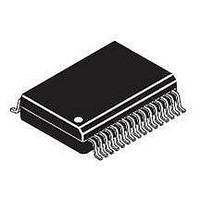
KIT33730EKEVBE Freescale Semiconductor, KIT33730EKEVBE Datasheet - Page 12

KIT33730EKEVBE
Manufacturer Part Number
KIT33730EKEVBE
Description
Power Management Modules & Development Tools SWITCH MODE PWR SUP
Manufacturer
Freescale Semiconductor
Type
Linear Regulators - Standardr
Datasheet
1.KIT33730EKEVBE.pdf
(26 pages)
Specifications of KIT33730EKEVBE
Product
Power Management Modules
Silicon Manufacturer
Freescale
Silicon Core Number
MC33730
Kit Application Type
Power Management
Application Sub Type
SMPS
Kit Contents
Board, CD
Rohs Compliant
Yes
For Use With/related Products
MC33730
Lead Free Status / RoHS Status
Lead free / RoHS Compliant
PROGRAMMING PIN 2 (P2)
reference voltage. The output voltage of the VDD3, VDDL
and VKAM regulators can be programmed by the P1, P2, and
P3 pins (see
PROGRAMMING PIN 3 (P3)
reference voltages. The output voltage of the VDD3, VDDL
and VKAM regulators can be programmed by the P1, P2, and
P3 pins (see
PROTECTION FET DRIVE (PFD)
output drive for the gate of the external Reverse Battery
Protection N-channel FET.
BOOTSTRAP (BOOT)
provides the supply power for the switching regulator high-
side drive.
SLEW-RATE (SR)
of the switching regulator can be adjusted by connecting this
pin to switch node (SW pin, slow slew-rate selection), BOOT
pin (fast slew-rate selection), or it can be left open (medium
slew-rate selection).
SWITCH NODE (SW)
power switch (N-channel MOSFET source).
BATTERY VOLTAGE SUPPLY (VBAT)
protection is recommended).
12
33730
FUNCTIONAL DESCRIPTION
FUNCTIONAL PIN DESCRIPTION
Programming Pin 2 for the VDD3, VDDL, and VKAM
Programming Pin 3 for the VDD3, VDDL, and VKAM
Reverse battery protection FET gate drive. This pin is an
This pin is connected to the bootstrap capacitor. It
Slew-rate Control of the switching regulator. The slew-rate
This pin is the source of the switching regulator internal
Voltage supply to the IC (external reverse battery
Table
Table
6).
6).
KEEP ALIVE SUPPLY (KA_VBAT)
battery protected. This input supplies power to the internal
supply and bias circuits that have to do with this VKAM and
other always-on supplies.
CHARGE PUMP (CP)
This charge pump provides the voltage needed to sufficiently
enhance the gates of the internal n-channel mosfets (VREF1,
VREF2, and VDDH) during the low battery condition.
KEEP ALIVE MEMORY (VKAM)
supplies power for the module Keep-Alive memory. This
output is always on, if the voltage at the KA_VBAT pin is
above 4.5 V.
VDD3
of VDD3 regulator external NPN pass transitory is connected
to this pin.
Standby regulator (see
VDD3 LINEAR REGULATOR BASE DRIVE
(VDD3_B)
regulator without the external pass transistor.This output
supplies current into the base of the regulator external pass
NPN transistor.
GROUND (GND)
VOLTAGE IGNITION (VIGN)
through an ignition switch. This pin is reverse battery
protected.
This pin is the keep alive supply input. This input is reverse
External reservoir capacitor of the internal charge pump.
Keep Alive Memory (standby) supply output. This output
This is a VDD3 regulator output feedback pin.The emitter
This pin can programmed to be the output of the VDD3
This pin can be used also as an additional standby
This pin is the ground pin of the integrated circuit.
This pin is the turn-on control input that is controlled
LINEAR REGULATOR (VDD3)
Analog Integrated Circuit Device Data
Table
6).
Freescale Semiconductor


