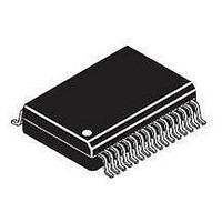
KIT33730EKEVBE Freescale Semiconductor, KIT33730EKEVBE Datasheet - Page 3

KIT33730EKEVBE
Manufacturer Part Number
KIT33730EKEVBE
Description
Power Management Modules & Development Tools SWITCH MODE PWR SUP
Manufacturer
Freescale Semiconductor
Type
Linear Regulators - Standardr
Datasheet
1.KIT33730EKEVBE.pdf
(26 pages)
Specifications of KIT33730EKEVBE
Product
Power Management Modules
Silicon Manufacturer
Freescale
Silicon Core Number
MC33730
Kit Application Type
Power Management
Application Sub Type
SMPS
Kit Contents
Board, CD
Rohs Compliant
Yes
For Use With/related Products
MC33730
Lead Free Status / RoHS Status
Lead free / RoHS Compliant
Table 1. 33730 Pin Definitions
Analog Integrated Circuit Device Data
Freescale Semiconductor
Pin Number
Note: The exposed pad is electrically and thermally connected to the IC ground.
A functional description of each pin can be found in the Functional Pin Description section beginning on
10
11
12
13
14
15
1
2
3
4
5
6
7
8
9
Pin Name
RSTKAM
VDDL_B
IGN_ON
REGON
VCOMP
VREF2
VREF1
RSTH
VDDH
FREQ
VDDL
RSTL
RST3
HRT
INV
Pin Function
Power Output
Power Output
Analog Input
Analog Input
Analog Input Frequency Adjustment Frequency adjustment of the switching regulator. The value of the resistor
Power Input
Open Drain
Open Drain
Open Drain
Open Drain
Open Drain
Logic Input
Analog/
Analog
Output
Analog
Output
Analog
Output
RSTKAM
VDDL_B
IGN_ON
REGON
VCOMP
VREF2
VREF1
Hardware Reset Timer This pin is the hardware reset timer programmed with an external resistor.
VDDL Regulator Base
VDDH
FREQ
RSTH
VDDL
RSTL
RST3
Regulator Hold On
HRT
VDDH Regulator
VDDL Regulator
INV
VREF Output 2
VREF Output 1
Formal Name
Compensation
Inverting Input
P1
VKAM Reset
VDDH Reset
VDDL Reset
VDD3 Reset
VIGN Status
Figure 3. 33730 Pin Connections
Drive
PIN CONNECTIONS
1
2
3
4
5
6
7
8
9
10
11
12
13
14
15
16
This pin is an open drain reset output, monitoring the V
microprocessor.
This pin is an open drain reset output, monitoring the V
This pin is an open drain reset output, monitoring the V
This pin is an open drain reset output, monitoring the V
This pin is the output of the protected supply VREF2. The pin is supplied
from the V
This pin is the V
This pin is the 5.0 V output feedback pin of the buck regulator. The pin is
also a power input for the protected outputs VREF1,2.
VDDL linear regulator base drive.
This pin is the output of the protected supply VREF1. The pin is supplied
from the V
Regulator Hold On input pin (5.0 V logic level input).
This open drain output signals the status of the VIGN pin.
This pin provides switching pre-regulator compensation, it is the output of
the error amplifier.
Inverting input of the switching regulator error amplifier.
to ground at this pin determines the oscillator frequency.
DDH
DDH
32
31
30
29
28
27
26
25
24
23
22
21
20
19
18
17
through the protection FET.
through the protection FET.
DDL
regulator output feedback pin.
P3
VIGN
GND
VDD3_B
VDD3
VKAM
CP
KA_VBAT
VBAT
VBAT
SW
SW
SR
BOOT
PFD
P2
Definition
page
PIN CONNECTIONS
KAM
DDH
DDL
DD3
11.
supply to the
regulator.
regulator.
regulator.
33730
3


