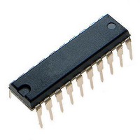
ATTINY461V-10PU Atmel, ATTINY461V-10PU Datasheet - Page 107

ATTINY461V-10PU
Manufacturer Part Number
ATTINY461V-10PU
Description
Microcontrollers (MCU) 4kB Flash 0.256kB EEPROM 16 I/O Pins
Manufacturer
Atmel
Specifications of ATTINY461V-10PU
Processor Series
ATTINY4x
Core
AVR8
Data Bus Width
8 bit
Data Ram Size
256 B
Interface Type
2-Wire/SPI/USI
Maximum Clock Frequency
10 MHz
Number Of Programmable I/os
16
Number Of Timers
2
Operating Supply Voltage
2.7 V to 5.5 V
Maximum Operating Temperature
+ 85 C
Mounting Style
Through Hole
Minimum Operating Temperature
- 40 C
On-chip Adc
11-ch x 10-bit
Program Memory Type
Flash
Program Memory Size
4 KB
Package / Case
PDIP-20
Package
20PDIP
Device Core
AVR
Family Name
ATtiny
Maximum Speed
10 MHz
Ram Size
256 Byte
Operating Temperature
-40 to 85 °C
Lead Free Status / RoHS Status
Lead free / RoHS Compliant
Available stocks
Company
Part Number
Manufacturer
Quantity
Price
Company:
Part Number:
ATTINY461V-10PU
Manufacturer:
ATMEL
Quantity:
6 223
- Current page: 107 of 242
- Download datasheet (5Mb)
12.10 Fault Protection Unit
2588E–AVR–08/10
Figure 12-17. Timer/Counter Timing Diagram, Setting of OCF1x, with Prescaler (f
Figure 12-18
Figure 12-18. Timer/Counter Timing Diagram, with Prescaler (f
The Timer/Counter1 incorporates a Fault Protection unit, which can be set to disable the PWM
output pins when an external event is triggered. The external signal indicating an event can be
applied via the external interrupt INT0 pin or, alternatively, via the analog-comparator unit. The
Fault Protection unit is illustrated in
directly a part of the Fault Protection unit are gray shaded.
Figure 12-19. Fault Protection Unit Block Diagram
Fault Protection mode is enabled by setting the Fault Protection Enable (FPEN1) bit and trig-
gered by a change in logic level at external interrupt pin (INT0). Alternatively, fault protection
mode can be triggered by the Analog Comparator Output (ACO).
When Fault Protection is triggered, the COM1x bits are cleared, Output Comparators are discon-
nected from the PWM output pins and PORTB register bits are connected to the PWM output
TCNTn
(clk
TCNTn
OCRnx
(clk
OCFnx
TOVn
clk
clk
clk
INT0
clk
PCK
PCK
PCK
Tn
PCK
Tn
/8)
/8)
Comparator
shows the setting of TOV1 in Phase and Frequency Correct PWM Mode.
Analog
ACO*
BOTTOM + 1
OCRnx - 1
FPAC1
Figure
Canceler
FPNC1
Noise
BOTTOM + 1
12-19. The elements of the block diagram that are not
OCRnx
OCRnx Value
FPES1
Detector
Edge
FPEN1
OCRnx + 1
clkT1
BOTTOM
/8)
FAULT_PROTECTION (Int. Req.)
Timer/Counter1
BOTTOM + 1
clkT1
OCRnx + 2
/8)
107
Related parts for ATTINY461V-10PU
Image
Part Number
Description
Manufacturer
Datasheet
Request
R

Part Number:
Description:
Manufacturer:
Atmel Corporation
Datasheet:

Part Number:
Description:
Manufacturer:
Atmel Corporation
Datasheet:

Part Number:
Description:
IC AVR MCU 4K 20MHZ 32-QFN
Manufacturer:
Atmel
Datasheet:

Part Number:
Description:
IC MCU AVR 4K FLASH 20MHZ 20SOIC
Manufacturer:
Atmel
Datasheet:

Part Number:
Description:
MCU AVR 4K FLASH 15MHZ 32-QFN
Manufacturer:
Atmel
Datasheet:

Part Number:
Description:
MCU AVR 4KB FLASH 15MHZ 32-VQFN
Manufacturer:
Atmel
Datasheet:

Part Number:
Description:
MCU AVR 4KB FLASH 20MHZ 20SOIC
Manufacturer:
Atmel
Datasheet:

Part Number:
Description:
IC MCU AVR 4K 20MHZ 32QFN
Manufacturer:
Atmel
Datasheet:

Part Number:
Description:
Microcontrollers (MCU) 4kB Flash 0.256kB EEPROM 16 I/O Pins
Manufacturer:
Atmel
Datasheet:

Part Number:
Description:
IC, MCU, 8BIT, 2K FLASH, 20SOIC
Manufacturer:
Atmel
Datasheet:


