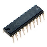
ATTINY461V-10PU Atmel, ATTINY461V-10PU Datasheet - Page 73

ATTINY461V-10PU
Manufacturer Part Number
ATTINY461V-10PU
Description
Microcontrollers (MCU) 4kB Flash 0.256kB EEPROM 16 I/O Pins
Manufacturer
Atmel
Specifications of ATTINY461V-10PU
Processor Series
ATTINY4x
Core
AVR8
Data Bus Width
8 bit
Data Ram Size
256 B
Interface Type
2-Wire/SPI/USI
Maximum Clock Frequency
10 MHz
Number Of Programmable I/os
16
Number Of Timers
2
Operating Supply Voltage
2.7 V to 5.5 V
Maximum Operating Temperature
+ 85 C
Mounting Style
Through Hole
Minimum Operating Temperature
- 40 C
On-chip Adc
11-ch x 10-bit
Program Memory Type
Flash
Program Memory Size
4 KB
Package / Case
PDIP-20
Package
20PDIP
Device Core
AVR
Family Name
ATtiny
Maximum Speed
10 MHz
Ram Size
256 Byte
Operating Temperature
-40 to 85 °C
Lead Free Status / RoHS Status
Lead free / RoHS Compliant
Available stocks
Company
Part Number
Manufacturer
Quantity
Price
Company:
Part Number:
ATTINY461V-10PU
Manufacturer:
ATMEL
Quantity:
6 223
- Current page: 73 of 242
- Download datasheet (5Mb)
11.3.1.1
11.3.2
2588E–AVR–08/10
External Clock Source
Prescaler Reset
Figure 11-2. Prescaler for Timer/Counter0
Note:
The prescaled clock has a frequency of f
Table 11-4 on page 85
The prescaler is free running, i.e. it operates independently of the Clock Select logic of the
Timer/Counter. Since the prescaler is not affected by the Timer/Counter’s clock select, the state
of the prescaler will have implications for situations where a prescaled clock is used. One exam-
ple of prescaling artifacts occurs when the timer is enabled and clocked by the prescaler (6 >
CSn2:0 > 1). The number of system clock cycles from when the timer is enabled to the first count
occurs can be from 1 to N+1 system clock cycles, where N equals the prescaler divisor (8, 64,
256, or 1024). It is possible to use the Prescaler Reset for synchronizing the Timer/Counter to
program execution.
An external clock source applied to the T0 pin can be used as Timer/Counter clock (clk
T0 pin is sampled once every system clock cycle by the pin synchronization logic. The synchro-
nized (sampled) signal is then passed through the edge detector.
equivalent block diagram of the T0 synchronization and edge detector logic. The registers are
clocked at the positive edge of the internal system clock (
high period of the internal system clock.
The edge detector generates one clk
= 6) edge it detects. See
PSR0
clk
T0
I/O
1. The synchronization logic on the input pins (
Synchronization
for details.
Table 11-4 on page 85
Clear
T
0
pulse for each positive (CSn2:0 = 7) or negative (CSn2:0
CLK_I/O
/8, f
for details.
T0)
CLK_I/O
is shown in
/64, f
clk
I/O
CLK_I/O
). The latch is transparent in the
Figure
Figure 11-3
/256, or f
11-3.
clk
T0
shows a functional
CLK_I/O
/1024. See
T0
). The
73
Related parts for ATTINY461V-10PU
Image
Part Number
Description
Manufacturer
Datasheet
Request
R

Part Number:
Description:
Manufacturer:
Atmel Corporation
Datasheet:

Part Number:
Description:
Manufacturer:
Atmel Corporation
Datasheet:

Part Number:
Description:
IC AVR MCU 4K 20MHZ 32-QFN
Manufacturer:
Atmel
Datasheet:

Part Number:
Description:
IC MCU AVR 4K FLASH 20MHZ 20SOIC
Manufacturer:
Atmel
Datasheet:

Part Number:
Description:
MCU AVR 4K FLASH 15MHZ 32-QFN
Manufacturer:
Atmel
Datasheet:

Part Number:
Description:
MCU AVR 4KB FLASH 15MHZ 32-VQFN
Manufacturer:
Atmel
Datasheet:

Part Number:
Description:
MCU AVR 4KB FLASH 20MHZ 20SOIC
Manufacturer:
Atmel
Datasheet:

Part Number:
Description:
IC MCU AVR 4K 20MHZ 32QFN
Manufacturer:
Atmel
Datasheet:

Part Number:
Description:
Microcontrollers (MCU) 4kB Flash 0.256kB EEPROM 16 I/O Pins
Manufacturer:
Atmel
Datasheet:

Part Number:
Description:
IC, MCU, 8BIT, 2K FLASH, 20SOIC
Manufacturer:
Atmel
Datasheet:


