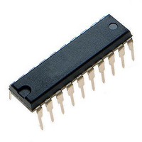
ATTINY461V-10PU Atmel, ATTINY461V-10PU Datasheet - Page 76

ATTINY461V-10PU
Manufacturer Part Number
ATTINY461V-10PU
Description
Microcontrollers (MCU) 4kB Flash 0.256kB EEPROM 16 I/O Pins
Manufacturer
Atmel
Specifications of ATTINY461V-10PU
Processor Series
ATTINY4x
Core
AVR8
Data Bus Width
8 bit
Data Ram Size
256 B
Interface Type
2-Wire/SPI/USI
Maximum Clock Frequency
10 MHz
Number Of Programmable I/os
16
Number Of Timers
2
Operating Supply Voltage
2.7 V to 5.5 V
Maximum Operating Temperature
+ 85 C
Mounting Style
Through Hole
Minimum Operating Temperature
- 40 C
On-chip Adc
11-ch x 10-bit
Program Memory Type
Flash
Program Memory Size
4 KB
Package / Case
PDIP-20
Package
20PDIP
Device Core
AVR
Family Name
ATtiny
Maximum Speed
10 MHz
Ram Size
256 Byte
Operating Temperature
-40 to 85 °C
Lead Free Status / RoHS Status
Lead free / RoHS Compliant
Available stocks
Company
Part Number
Manufacturer
Quantity
Price
Company:
Part Number:
ATTINY461V-10PU
Manufacturer:
ATMEL
Quantity:
6 223
- Current page: 76 of 242
- Download datasheet (5Mb)
11.5.1
11.5.2
11.5.3
11.6
76
Output Compare Unit
ATtiny261/461/861
Input Capture Trigger Source
Noise Canceler
Using the Input Capture Unit
the same system clock as the TCNT0 value is copied into Input Capture Register. If enabled
(TICIE0=1), the Input Capture Flag generates an Input Capture interrupt. The ICF0 flag is auto-
matically cleared when the interrupt is executed. Alternatively the ICF0 flag can be cleared by
software by writing a logical one to its I/O bit location.
The default trigger source for the Input Capture unit is the Input Capture pin (ICP0).
Timer/Counter0 can alternatively use the Analog Comparator output as trigger source for the
Input Capture unit. The Analog Comparator is selected as trigger source by setting the Analog
Comparator Input Capture Enable (ACIC0) bit in the Timer/Counter Control Register A
(TCCR0A). Be aware that changing trigger source can trigger a capture. The Input Capture Flag
must therefore be cleared after the change.
Both the Input Capture pin (ICP0) and the Analog Comparator output (ACO) inputs are sampled
using the same technique as for the T0 pin
identical. However, when the noise canceler is enabled, additional logic is inserted before the
edge detector, which increases the delay by four system clock cycles. An Input Capture can also
be triggered by software by controlling the port of the ICP0 pin.
The noise canceler improves noise immunity by using a simple digital filtering scheme. The
noise canceler input is monitored over four samples, and all four must be equal for changing the
output that in turn is used by the edge detector.
The noise canceler is enabled by setting the Input Capture Noise Canceler (ICNC0) bit in
Timer/Counter Control Register B (TCCR0B). When enabled the noise canceler introduces addi-
tional four system clock cycles of delay from a change applied to the input, to the update of the
ICR0 Register. The noise canceler uses the system clock and is therefore not affected by the
prescaler.
The main challenge when using the Input Capture unit is to assign enough processor capacity
for handling the incoming events. The time between two events is critical. If the processor has
not read the captured value in the ICR0 Register before the next event occurs, the ICR0 will be
overwritten with a new value. In this case the result of the capture will be incorrect.
When using the Input Capture interrupt, the ICR0 Register should be read as early in the inter-
rupt handler routine as possible. The maximum interrupt response time is dependent on the
maximum number of clock cycles it takes to handle any of the other interrupt requests.
Measurement of an external signal’s duty cycle requires that the trigger edge is changed after
each capture. Changing the edge sensing must be done as early as possible after the ICR0
Register has been read. After a change of the edge, the Input Capture Flag (ICF0) must be
cleared by software (writing a logical one to the I/O bit location). For measuring frequency only,
the trigger edge change is not required (if an interrupt handler is used).
The comparator continuously compares Timer/Counter (TCNT0) with the Output Compare Reg-
isters (OCR0A and OCR0B), and whenever the Timer/Counter equals to the Output Compare
Regisers, the comparator signals a match. A match will set the Output Compare Flag at the next
timer clock cycle. In 8-bit mode the match can set either the Output Compare Flag OCF0A or
(Figure 11-4 on page
85). The edge detector is also
2588E–AVR–08/10
Related parts for ATTINY461V-10PU
Image
Part Number
Description
Manufacturer
Datasheet
Request
R

Part Number:
Description:
Manufacturer:
Atmel Corporation
Datasheet:

Part Number:
Description:
Manufacturer:
Atmel Corporation
Datasheet:

Part Number:
Description:
IC AVR MCU 4K 20MHZ 32-QFN
Manufacturer:
Atmel
Datasheet:

Part Number:
Description:
IC MCU AVR 4K FLASH 20MHZ 20SOIC
Manufacturer:
Atmel
Datasheet:

Part Number:
Description:
MCU AVR 4K FLASH 15MHZ 32-QFN
Manufacturer:
Atmel
Datasheet:

Part Number:
Description:
MCU AVR 4KB FLASH 15MHZ 32-VQFN
Manufacturer:
Atmel
Datasheet:

Part Number:
Description:
MCU AVR 4KB FLASH 20MHZ 20SOIC
Manufacturer:
Atmel
Datasheet:

Part Number:
Description:
IC MCU AVR 4K 20MHZ 32QFN
Manufacturer:
Atmel
Datasheet:

Part Number:
Description:
Microcontrollers (MCU) 4kB Flash 0.256kB EEPROM 16 I/O Pins
Manufacturer:
Atmel
Datasheet:

Part Number:
Description:
IC, MCU, 8BIT, 2K FLASH, 20SOIC
Manufacturer:
Atmel
Datasheet:


