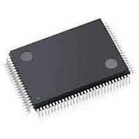
APA150-TQG100 Actel, APA150-TQG100 Datasheet - Page 20

APA150-TQG100
Manufacturer Part Number
APA150-TQG100
Description
FPGA - Field Programmable Gate Array 150K System Gates
Manufacturer
Actel
Datasheet
1.APA075-FGG144.pdf
(178 pages)
Specifications of APA150-TQG100
Processor Series
APA150
Core
IP Core
Maximum Operating Frequency
150 MHz
Number Of Programmable I/os
242
Data Ram Size
36864
Supply Voltage (max)
2.7 V
Maximum Operating Temperature
+ 70 C
Minimum Operating Temperature
0 C
Development Tools By Supplier
APA-Eval-Kit, APA-Eval-BRD1, Silicon-Explorer II, Silicon-Sculptor 3, SI-EX-TCA, Flashpro 4, Flashpro 3, Flashpro Lite
Mounting Style
SMD/SMT
Supply Voltage (min)
2.3 V
Number Of Gates
150 K
Package / Case
TQFP-100
Lead Free Status / RoHS Status
Lead free / RoHS Compliant
Available stocks
Company
Part Number
Manufacturer
Quantity
Price
Company:
Part Number:
APA150-TQG100A
Manufacturer:
Microsemi SoC
Quantity:
10 000
Company:
Part Number:
APA150-TQG100I
Manufacturer:
LT
Quantity:
1 400
Company:
Part Number:
APA150-TQG100I
Manufacturer:
Microsemi SoC
Quantity:
10 000
Timing Control and
Characteristics
ProASIC
ProASIC
clock conditioning capabilities. Each member of the
ProASIC
blocks which perform the following functions:
Each PLL has the following key features:
Note: Jitter (ps) = Jitter (%) × period
For Example:
Physical Implementation
Each side of the chip contains a clock conditioning circuit
based on a 180 MHz PLL block
2-11). Two global multiplexed lines extend along each
side of the chip to provide bidirectional access to the PLL
on that side (neither MUX can be connected to the
opposite side's PLL). Each global line has optional LVPECL
input pads (described below). The global lines may be
driven by either the LVPECL global input pad or the
outputs from the PLL block, or both. Each global line can
be driven by a different output from the PLL. Unused
global pins can be configured as regular I/Os or left
unconnected. They default to an input with pull-up. The
two signals available to drive the global networks are as
2 -1 0
Jitter in picoseconds at 100 MHz = 0.01 × (1/100E6) = 100 ps
ProASIC
• Clock Phase Adjustment via Programmable Delay
• Clock Skew Minimization
• Clock Frequency Synthesis
• Input Frequency Range (f
• Feedback Frequency Range (f
• Output Frequency Range (f
• Output Phase Shift = 0 ° and 180 °
• Output Duty Cycle = 50%
• Low Output Jitter (maximum at 25°C)
• Low Power Consumption – 6.9 mW (max. – analog
• Maximum Acquisition
1. This mode is available through the delay feature of the global MUX driver.
(250 ps steps from –7 ns to +8 ns)
– f
– 10 MHz < f
– f
supply) + 7.0 µW/MHz (max. – digital supply)
Time
PLUS
PLUS
PLUS
VCO
VCO
PLUS
devices provide designers with very flexible
family contains two phase-locked loop (PLL)
Flash Family FPGAs
<10 MHz. Jitter ±1% or better
> 60 MHz. Jitter ±1% or better
Clock Management System
VCO
< 60 MHz. Jitter ±2% or better
= 80 µs for f
= 30 µs for f
IN
) = 1.5 to 180 MHz
OUT
(Figure 2-11 on page
VCO
) = 8 to 180 MHz
) = 24 to 180 MHz
VCO
VCO
> 40 MHz
< 40 MHz
v5.9
follows
12, and
Global A (secondary clock)
Global B
Functional Description
Each PLL block contains four programmable dividers as
shown in
frequency scaling of the input clock signal as follows:
The implementations shown in
the user to define a wide range of frequency multiplier
and divisors.
• Output from Global MUX A
• Conditioned version of PLL output (f
• Divided version of either of the above
• Further delayed version of either of the above
• Output from Global MUX B
• Delayed or advanced version of f
• Divided version of either of the above
• Further delayed version of either of the above
• The n divider divides the input clock by integer
• The m divider in the feedback path allows
• The two dividers together can implement any
• The output frequency of the PLL core is given by
• The third and fourth dividers (u and v) permit the
f
OUT
or advanced
(0.25 ns, 0.50 ns, or 4.00 ns delay)
(0.25 ns, 0.50 ns, or 4.00 ns delay)
factors from 1 to 32.
multiplication of the input clock by integer factors
ranging from 1 to 64.
combination
resulting in a clock frequency between 24 and 180
MHz exiting the PLL core. This clock has a fixed
50% duty cycle.
the formula in
frequency):
signals applied to the global network to each be
further divided by integer factors ranging from 1
to 4.
Table 2-8 on page
(Figure 2-12 on page
= f
REF
Figure 2-11 on page
× m ÷ n
of
f
f
EQ 2-1
GLB
GLA
2-13):
multiplication
=
=
-----------------
(
---------------- -
(
n u
n v
(f
2-12,
m
m
×
REF
×
EQ 2-2
)
)
is the reference clock
Table 2-7 on page 2-
2-11. These allow
and
OUT
1
2
OUT
and
EQ 2-3
) – delayed
division
enable
EQ 2-1
EQ 2-2
EQ 2-3


