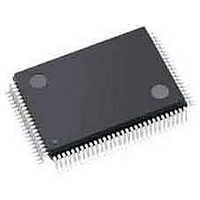
APA150-TQG100 Actel, APA150-TQG100 Datasheet - Page 72

APA150-TQG100
Manufacturer Part Number
APA150-TQG100
Description
FPGA - Field Programmable Gate Array 150K System Gates
Manufacturer
Actel
Datasheet
1.APA075-FGG144.pdf
(178 pages)
Specifications of APA150-TQG100
Processor Series
APA150
Core
IP Core
Maximum Operating Frequency
150 MHz
Number Of Programmable I/os
242
Data Ram Size
36864
Supply Voltage (max)
2.7 V
Maximum Operating Temperature
+ 70 C
Minimum Operating Temperature
0 C
Development Tools By Supplier
APA-Eval-Kit, APA-Eval-BRD1, Silicon-Explorer II, Silicon-Sculptor 3, SI-EX-TCA, Flashpro 4, Flashpro 3, Flashpro Lite
Mounting Style
SMD/SMT
Supply Voltage (min)
2.3 V
Number Of Gates
150 K
Package / Case
TQFP-100
Lead Free Status / RoHS Status
Lead free / RoHS Compliant
Available stocks
Company
Part Number
Manufacturer
Quantity
Price
Company:
Part Number:
APA150-TQG100A
Manufacturer:
Microsemi SoC
Quantity:
10 000
Company:
Part Number:
APA150-TQG100I
Manufacturer:
LT
Quantity:
1 400
Company:
Part Number:
APA150-TQG100I
Manufacturer:
Microsemi SoC
Quantity:
10 000
Asynchronous Write and Synchronous Read to the Same Location
Note: *New data is read if WB
Figure 2-35 • Asynchronous Write and Synchronous Read to the Same Location
Table 2-59 • T
2 -6 2
Symbol t
CCYC
CMH
CML
WBRCLKS
WBRCLKH
OCH
OCA
DWRRCLKS
DWRH
Notes:
1. This behavior is valid for Access Timed Output and Pipelined Mode Output. The table shows the timings of an Access Timed Output.
2. In asynchronous write and synchronous read access to the same location, the new write data will be read out if the active write
3. A setup or hold time violation will result in unknown output data.
ProASIC
signal edge occurs before or at the same time as the active read clock edge. If WB changes to low after hold time, the data will be
read.
normal operation status.
PLUS
xxx
T
J
J
WB = {WRB + WBLKB}
Flash Family FPGAs
= 0°C to 110°C; V
= –55°C to 150°C, V
Cycle time
Clock high phase
Clock low phase
WB ↓ to RCLKS ↑ setup time
WB ↓ to RCLKS ↑ hold time
Old DO valid from RCLKS ↑
New DO valid from RCLKS ↑
DI to RCLKS ↑ setup time
DI to WB ↑ hold time
RCLKS
↓
t
DO
DD
DWRRCLK
Description
occurs before setup time. The stored data is read if WB
DI
t
t
BRCLKH
DD
WRCKS
= 2.3 V to 2.7 V for Commercial/Industrial
t
t
OCH
Last Cycle Data
OCA
= 2.3 V to 2.7 V for Military/MIL-STD-883
t
CMH
v5.9
Min.
–0.1
7.5
3.0
3.0
7.5
0
t
CCYC
Max.
t
CML
7.0
3.0
1.5
t
DWRH
↓
occurs after hold time. The plot shows the
Units
ns
ns
ns
ns
ns
ns
ns
ns
ns
New Data*
OCA/OCH
Access Timed Output
Notes
displayed
for


