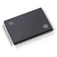
APA150-TQG100 Actel, APA150-TQG100 Datasheet - Page 27

APA150-TQG100
Manufacturer Part Number
APA150-TQG100
Description
FPGA - Field Programmable Gate Array 150K System Gates
Manufacturer
Actel
Datasheet
1.APA075-FGG144.pdf
(178 pages)
Specifications of APA150-TQG100
Processor Series
APA150
Core
IP Core
Maximum Operating Frequency
150 MHz
Number Of Programmable I/os
242
Data Ram Size
36864
Supply Voltage (max)
2.7 V
Maximum Operating Temperature
+ 70 C
Minimum Operating Temperature
0 C
Development Tools By Supplier
APA-Eval-Kit, APA-Eval-BRD1, Silicon-Explorer II, Silicon-Sculptor 3, SI-EX-TCA, Flashpro 4, Flashpro 3, Flashpro Lite
Mounting Style
SMD/SMT
Supply Voltage (min)
2.3 V
Number Of Gates
150 K
Package / Case
TQFP-100
Lead Free Status / RoHS Status
Lead free / RoHS Compliant
Available stocks
Company
Part Number
Manufacturer
Quantity
Price
Company:
Part Number:
APA150-TQG100A
Manufacturer:
Microsemi SoC
Quantity:
10 000
Company:
Part Number:
APA150-TQG100I
Manufacturer:
LT
Quantity:
1 400
Company:
Part Number:
APA150-TQG100I
Manufacturer:
Microsemi SoC
Quantity:
10 000
Logic Tile Timing Characteristics
Timing characteristics for ProASIC
three categories: family dependent, device dependent,
and design dependent. The input and output buffer
characteristics are common to all ProASIC
members. Internal routing delays are device dependent.
Design dependency means that actual delays are not
determined until after placement and routing of the
user’s design are complete. Delay values may then be
determined by using the Timer utility or by performing
simulation with post-layout delays.
Critical Nets and Typical Nets
Propagation delays are expressed only for typical nets,
which are used for initial design performance evaluation.
Critical net delays can then be applied to the most
timing-critical paths. Critical nets are determined by net
property assignment prior to place-and-route. Refer to
the Actel
on using constraints.
Table 2-9 •
2.3 V
2.5 V
2.7 V
Notes:
1. The user can set the junction temperature in Designer software to be any integer value in the range of –55°C to 175°C.
2. The user can set the core voltage in Designer software to be any value between 1.4 V and 1.6 V.
Designer User’s Guide
Temperature and Voltage Derating Factors
(Normalized to Worst-Case Commercial, T
–55°C
0.84
0.81
0.77
–40°C
0.86
0.82
0.79
or online help for details
PLUS
0.91
0.87
0.83
0°C
devices fall into
PLUS
25°C
0.94
0.90
0.86
family
J
= 70°C, V
70°C
1.00
0.95
0.91
v5.9
Timing Derating
Since ProASIC
CMOS process, device performance will vary with
temperature, voltage, and process. Minimum timing
parameters
minimum operating temperature, and optimal process
variations. Maximum timing parameters reflect minimum
operating voltage, maximum operating temperature,
and worst-case process variations (within process
specifications). The derating factors shown in
should be applied to all timing data contained within
this datasheet.
All timing numbers listed in this datasheet represent
sample timing characteristics of ProASIC
Actual timing delay values are design-specific and can be
derived from the Timer tool in Actel’s Designer software
after place-and-route.
DD
= 2.3 V)
85°C
1.02
0.98
0.93
reflect
PLUS
110°C
1.05
1.01
0.96
devices are manufactured with a
maximum
ProASIC
125°C
1.13
1.09
1.04
PLUS
operating
Flash Family FPGAs
135°C
1.18
1.13
1.08
PLUS
Table 2-9
150°C
voltage,
devices.
1.27
1.21
1.16
2-17


