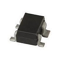
BFG25AW/X,115 NXP Semiconductors, BFG25AW/X,115 Datasheet - Page 2

BFG25AW/X,115
Manufacturer Part Number
BFG25AW/X,115
Description
TRANS RF NPN 5GHZ 5V SOT343
Manufacturer
NXP Semiconductors
Datasheet
1.BFG25AWX115.pdf
(14 pages)
Specifications of BFG25AW/X,115
Package / Case
SOT-343N
Transistor Type
NPN
Voltage - Collector Emitter Breakdown (max)
5V
Frequency - Transition
5GHz
Noise Figure (db Typ @ F)
1.9dB ~ 2dB @1GHz
Power - Max
500mW
Dc Current Gain (hfe) (min) @ Ic, Vce
50 @ 500µA, 1V
Current - Collector (ic) (max)
6.5mA
Mounting Type
Surface Mount
Dc Collector/base Gain Hfe Min
50
Dc Current Gain Hfe Max
200
Mounting Style
SMD/SMT
Configuration
Single
Transistor Polarity
NPN
Collector- Emitter Voltage Vceo Max
5 V
Emitter- Base Voltage Vebo
2 V
Continuous Collector Current
6.5 mA
Power Dissipation
500 mW
Lead Free Status / RoHS Status
Lead free / RoHS Compliant
Gain
-
Lead Free Status / RoHS Status
Lead free / RoHS Compliant, Lead free / RoHS Compliant
Other names
568-6185-2
BFG25AW/X,115
BFG25AW/X,115
NXP Semiconductors
FEATURES
Low current consumption
Low noise figure
Gold metallization ensures
APPLICATIONS
Wideband applications in UHF low
power amplifiers, such as pocket
telephones and paging systems.
DESCRIPTION
NPN silicon planar epitaxial transistor
in a 4-pin dual-emitter SOT343N
plastic package.
QUICK REFERENCE DATA
LIMITING VALUES
In accordance with the Absolute Maximum Rating System (IEC 134).
Note
1. T
1998 Sep 23
V
V
I
P
h
C
f
G
F
V
V
V
I
P
T
T
SYMBOL
SYMBOL
C
T
C
FE
(100 A to 1 mA)
excellent reliability.
stg
j
CBO
CEO
tot
CBO
CEO
EBO
tot
NPN 5 GHz wideband transistors
re
UM
s
is the temperature at the soldering point of the collector pin.
collector-base voltage
collector-emitter voltage
collector current (DC)
total power dissipation
DC current gain
feedback capacitance
transition frequency
maximum unilateral
power gain
noise figure
collector-base voltage
collector-emitter voltage
emitter-base voltage
collector current (DC)
total power dissipation
storage temperature
junction temperature
PARAMETER
PARAMETER
open emitter
open base
T
I
I
I
I
C
C
C
C
PINNING
s
s
BFG25AW
BFG25AW/X
= 0.5 mA; V
= 0; V
= 1 mA; V
= 0.5 mA; V
85 C
PIN
1
2
3
4
1
2
3
4
opt
; I
CE
open emitter
open base
open collector
T
C
s
= 1 V; f = 1 MHz
= 1 mA; V
collector
base
emitter
emitter
collector
emitter
base
emitter
CE
85 C; see Fig.2; note 1
CE
CE
= 1 V; f = 500 MHz; T
CONDITIONS
= 1 V
= 1 V; f = 1 GHz; T
DESCRIPTION
2
CE
CONDITIONS
= 1 V; f = 1 GHz
amb
amb
= 25 C
= 25 C 3.5
lfpage
MARKING
BFG25AW
BFG25AW/X
TYPE NUMBER
50
65
MIN.
MIN.
Fig.1 SOT343N.
4
1
Top view
Product specification
BFG25AW/X
80
0.2
5
16
2
TYP. MAX. UNIT
BFG25AW;
8
5
2
6.5
500
+150
175
MAX.
8
5
6.5
500
200
0.3
3
2
CODE
MBK523
N6
V1
V
V
V
mA
mW
C
C
UNIT
V
V
mA
mW
pF
GHz
dB
dB


