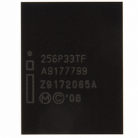
RC28F256P33TFA NUMONYX, RC28F256P33TFA Datasheet - Page 11

RC28F256P33TFA
Manufacturer Part Number
RC28F256P33TFA
Description
IC FLASH 256MBIT 95NS 64EZBGA
Manufacturer
NUMONYX
Series
Axcell™r
Specifications of RC28F256P33TFA
Format - Memory
FLASH
Memory Type
FLASH
Memory Size
256M (16Mx16)
Speed
95ns
Interface
Parallel
Voltage - Supply
2.3 V ~ 3.6 V
Operating Temperature
-40°C ~ 85°C
Package / Case
64-EZBGA
Cell Type
NOR
Density
256Mb
Interface Type
Parallel/Serial
Boot Type
Top
Address Bus
25b
Operating Supply Voltage (typ)
2.5/3/3.3V
Operating Temp Range
-40C to 85C
Package Type
EZBGA
Sync/async
Async/Sync
Operating Temperature Classification
Industrial
Operating Supply Voltage (min)
2.3V
Operating Supply Voltage (max)
3.6V
Word Size
16b
Number Of Words
32M
Supply Current
50mA
Mounting
Surface Mount
Pin Count
64
Lead Free Status / RoHS Status
Contains lead / RoHS non-compliant
Other names
902063
902063
RC28F256P33TF 902063
902063
RC28F256P33TF 902063
Available stocks
Company
Part Number
Manufacturer
Quantity
Price
Company:
Part Number:
RC28F256P33TFA
Manufacturer:
Micron Technology Inc
Quantity:
10 000
Conversion Guide: P33 130nm to 65nm
5.0
5.1
Table 6:
5.2
Note:
Application Note
11
Device Identification
Code Type
P33 Device ID Codes
Flash Software Design Considerations
The following sections discuss software design considerations when converting from the
P33 130nm device to the P33 65nm device.
Device Identification
The P33 130nm and P33 65nm flash devices have identical device identification codes.
Read Configuration Register (RCR)
Read configurations for both the P33 130nm and P33 65nm devices are configured
using the Read Configuration Register (RCR). For example, to place the device in
synchronous burst-read mode, you set the read mode bit in the RCR. The P33 65nm
RCR includes the following modifications to the RCR:
• Latency Count RCR[14:11]: an additional bit, RCR14, has been added to the P33
• WAIT Polarity RCR[10]: P33 130nm default setting high and P33 65nm default
• Data Hold RCR[9]: P33 130nm supports 1-clock or 2-clock cycle data hold. RCR[9] is
• WAIT Delay RCR[8]: Same values for P33 130nm and P33-65nm.
• Burst Sequence RCR[7]: P33 130nm supports Linear “1” and Intel “0” burst order.
• Clock Edge RCR[6]: Same values for P33 130nm and P33 65nm.
• Reserved RCR[5:4]: Same values for P33 130nm and P33 65nm.
• Burst Wrap RCR[3]: Same values for P33 130nm and P33 65nm.
• Burst Length RCR[2:0]: Same values for P33 130nm and P33 65nm.
The differences are summarized in the table below.
65nm device; RCR14 was reserved on P33 130nm. P33 65nm supports latency
counts of 8, 9, 10, 11, 12, 13, 14, and 15.
setting is low.
reserved for P33 65nm and supports a data hold of one cycle only.
P33 65nm supports linear “0” only. Setting P33 65nm to “1” will not affect the burst
order; the burst order will always be linear.
Address
Offset
0x01
256 Mbit
Density
Device
891F
Top
P33-130nm Codes
Bottom
8922
891F
Top
P33-65nm Codes
Order Number: 320005-04
Bottom
8922
Sep 2008


