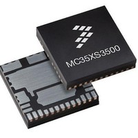
MC35XS3500PNA Freescale Semiconductor, MC35XS3500PNA Datasheet - Page 19

MC35XS3500PNA
Manufacturer Part Number
MC35XS3500PNA
Description
IC SWITCH HIGHSIDE 24PQFN
Manufacturer
Freescale Semiconductor
Type
High Side Switchr
Datasheet
1.MC35XS3500PNAR2.pdf
(41 pages)
Specifications of MC35XS3500PNA
Number Of Outputs
5
Rds (on)
*
Internal Switch(s)
Yes
Current Limit
9A
Voltage - Input
7 V ~ 20 V
Operating Temperature
-40°C ~ 125°C
Mounting Type
Surface Mount
Package / Case
24-PQFN, 24-PowerQFN
Product
MOSFET Gate Drivers
Rise Time
50 ns
Fall Time
50 ns
Propagation Delay Time
6.5 ms
Supply Voltage (max)
+ 5.5 V
Supply Voltage (min)
- 0.3 V
Supply Current
20 mA
Maximum Operating Temperature
+ 125
Minimum Operating Temperature
- 40 C
Lead Free Status / RoHS Status
Lead free / RoHS Compliant
Available stocks
Company
Part Number
Manufacturer
Quantity
Price
the Fail mode can be activated by a logic high signal at the
input.
Ignition Input (IGN)
Fail Home mode activation. The signal is “high active”,
meaning the component is active in case of a logic high at the
input.
Flasher Input (FLASHER)
Fail mode activation. The signal is “high active”, meaning the
component is active in case of a logic high at the input.
Reset Input (RST)
logic [1]. It is also used to initialize the device configuration
and the SPI fault registers when the signal is low. All SI/SO
registers described in
fault management is not affected by RST (see
Current Sense Output (CSNS)
a voltage proportional to the temperature on the GND flag.
The routing to the common resistor is SPI programmable.
case of the OUT6 is not used. So, the current sense
monitoring can be synchronized with a rising edge on the
FETOUT pin (t
[1]. Connection of the FETOUT-pin to a MCU input pin allows
the MCU to sample the CSNS-pin during a valid time-slot.
Since this falling edge is generated at the end of this time-
slot, upon a switch-off command, this feature may be used to
implement maximum current control.
Charge Pump (CP)
the VBAT pin. It is used as a tank for the internal charge
pump. Its typical value is 100 nF ± 20%, 25 V maximum.
Analog Integrated Circuit Device Data
Freescale Semiconductor
The Ignition input wakes the device. It also controls the
The Flasher input wakes the device. It also controls the
This input wakes the device when the RST pin is at
The current sense output pin is an analog current output or
This current sense monitoring may be synchronized in
An external capacitor is connected between this pin and
CSNS(SYNC)
Table 8
) if CSNS sync SPI bit is set to logic
and
Table 11
are reset. The
Figure
2).
FETOUT Output (FETOUT)
(OUT6).
V
voltage on V
FETIN Input (FETIN)
MOSFET. It can be routed on the CSNS output by a SPI
command.
SPI Protocol Description
synchronous data transfer with four I /O lines associated with
it: Serial Clock (SCLK), Serial Input (SI), Serial Output (SO),
and Chip Select (CS).
first-out (D15 to D0) protocol, with both input and output
words transferring the most significant bit (MSB) first. All
inputs are compatible with 5.0V CMOS logic levels supplied
by V
Serial Clock (SCLK)
35XS3500 device. The SI pin accepts data into the input shift
register on the falling edge of the SCLK signal, while the SO
pin shifts data information out of the SO line driver on the
rising edge of the SCLK signal. It is important that the SCLK
pin be in a logic low state whenever CS makes any transition.
For this reason, it is recommended that the SCLK pin be in a
logic [0] whenever the device is not accessed (CS logic [1]
state). SCLK has a passive pull-down, R
logic [1], signals at the SCLK and SI pins are ignored and SO
is tri-stated (high-impedance) (see
CC
This output pin is used to control an external MOSFET
The high level of the FETOUT Output is VCC if V
FETOUT is not protected in case of a short circuit or under-
In case of a reverse battery, OUT6 is OFF.
This input pin gives the current recopy of the external
The SPI interface has a full-duplex, three-wire
The SI/SO pins of the 35XS3500 device follow a first-in,
The SPI lines perform the following functions:
The SCLK pin clocks the internal shift registers of the
CC
are available in case of FETOUT is controlled ON.
.
BAT
.
FUNCTIONAL PIN DESCRIPTION
FUNCTIONAL DESCRIPTION
Figure
DWN
8).
. When CS is
35XS3500
BAT
and
19


