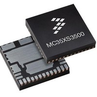
MC35XS3500PNA Freescale Semiconductor, MC35XS3500PNA Datasheet - Page 29

MC35XS3500PNA
Manufacturer Part Number
MC35XS3500PNA
Description
IC SWITCH HIGHSIDE 24PQFN
Manufacturer
Freescale Semiconductor
Type
High Side Switchr
Datasheet
1.MC35XS3500PNAR2.pdf
(41 pages)
Specifications of MC35XS3500PNA
Number Of Outputs
5
Rds (on)
*
Internal Switch(s)
Yes
Current Limit
9A
Voltage - Input
7 V ~ 20 V
Operating Temperature
-40°C ~ 125°C
Mounting Type
Surface Mount
Package / Case
24-PQFN, 24-PowerQFN
Product
MOSFET Gate Drivers
Rise Time
50 ns
Fall Time
50 ns
Propagation Delay Time
6.5 ms
Supply Voltage (max)
+ 5.5 V
Supply Voltage (min)
- 0.3 V
Supply Current
20 mA
Maximum Operating Temperature
+ 125
Minimum Operating Temperature
- 40 C
Lead Free Status / RoHS Status
Lead free / RoHS Compliant
Available stocks
Company
Part Number
Manufacturer
Quantity
Price
Previous Address SOA[1:0] = 11
status of the 35XS3500
Protection and Diagnosis
Output Protection Features
Over-temperature detection
each output (OUT1:OUT5 ). It can occur when the output pin
is in the ON or OFF state. An over-temperature fault condition
results in turning OFF the corresponding output. The fault is
latched and reported via the SPI. To delatch the fault and be
able to turn the outputs ON again, the failure condition must
be removed (T< 175 °C typically) and:
operation.
Over-current detections
(see
Analog Integrated Circuit Device Data
Freescale Semiconductor
OD15
OD13 (UVF) = Under-voltage Flag on Vbat
OD12 (OTW) = Over-temperature Prewarning Flag
OD11 (OTS) = Over-temperature Flag for all outputs
OD10 (NM) = Normal mode
OD4 (OUT5) = Logic [0] indicates the OUT5 voltage is lower than
V
V
If the previous two LSBs are 11, bits OD15 : OD0 reflect the
OUT_TH
OUT_TH
The 35XS3500 provides the following protection features:
• Protection against transients on V
• Active clamp, including protection against negative
• Over-temperature
• Severe and resistive Over-current
• Open Load during ON state
These protections are provided for each output (OUT1:5).
The 35XS3500 provides over-temperature shutdown for
• if the device was in Normal mode, the output
• if the device was in Fail mode, the corresponding output
The SPI fault report (OTS bit) is removed after a read
The 35XS3500 provides intelligent over-current shutdown
1
Figure
ISO 7637)
transients on output line
corresponding register (bit D7) must be rewritten.
Application of the complete OCHI window
(OCHI1+OCHI2 during t2) depends on toggling or not
toggling D7 bit.
is locked until device restart: wake up from Sleep mode
or V
OD14
. Logic [1] indicates the OUT5 voltage is higher than
BATPOR1
1
12) in order to protect the internal power
OD13
UVF
.
(Table
OD12
OTW
14).
OD11
OTS
BAT
OD10
NM
supply line (per
OD9
0
Table 15. Output Status
OD8
0
OD3 (OUT4) = Logic [0] indicates the OUT4 voltage is lower than
V
OD2 (OUT3) = Logic [0] indicates the OUT3 voltage is lower than
V
OD1 (OUT2) = Logic [0] indicates the OUT2 voltage is lower than
V
OD0 (OUT1) = Logic [0] indicates the OUT5 voltage is lower than
V
OD7
OUT_TH
OUT_TH
OUT_TH
OUT_TH
X
transistors and the harness in the event of overload (fuse
characteristic).
toggling the D7 bit in Normal mode. During the output
switching, the severe short-circuit condition provided on the
module connector is reported as an OCHI fault. In Fail mode,
the control of OCHI window is provided by the toggles:
IGN_ON, Flasher_ON. The current thresholds (I
and I
driver. After t
steady state. t
duration (t
in PWM mode during the inrush period, the t
to the sum of each “on” state duration in order to expand
dynamically the transient overcurrent profile.
detection), the corresponding output is disabled immediately.
The fault is latched and the status is reported via the SPI. To
delatch the fault, the failure condition must be removed and:
Figure 12. Double Over-current Window in Normal Mode
Output current
OCHI1
OCHI2
OCHI (I
In case of an overload (OCHI1 or OCHI2 or OCLO
For OCHI1:
• if the device was in Normal mode: the output
OCLO
OCLO
. Logic [1] indicates the OUT4 voltage is higher than V
. Logic [1] indicates the OUT3 voltage is higher than V
. Logic [1] indicates the OUT2 voltage is higher than V
. Logic [1] indicates the OUT1 voltage is higher than V
OD6
corresponding register (bit D7) must be rewritten D7=1.
X
) and the time (t
t1
ON
OCHI1
2,
) of the output. In case of the output is controlled
OD5
1
X
the OCLO current threshold is set to protect in
and t
and then I
t2
OUT5
2
OD4
times are compared to “on” state
LOGIC COMMANDS AND REGISTERS
1
FUNCTIONAL DEVICE OPERATION
OCHI2
and t
OUT4
OD3
2
) is only activated after
) are fixed numbers for each
OUT3
OD2
ON
OUT2
OD1
OCHI1
corresponds
35XS3500
OUT_TH
OUT_TH
OUT_TH
OUT_TH
, I
OUT1
time
OD0
OCHI2
29


