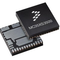
MC35XS3500PNA Freescale Semiconductor, MC35XS3500PNA Datasheet - Page 33

MC35XS3500PNA
Manufacturer Part Number
MC35XS3500PNA
Description
IC SWITCH HIGHSIDE 24PQFN
Manufacturer
Freescale Semiconductor
Type
High Side Switchr
Datasheet
1.MC35XS3500PNAR2.pdf
(41 pages)
Specifications of MC35XS3500PNA
Number Of Outputs
5
Rds (on)
*
Internal Switch(s)
Yes
Current Limit
9A
Voltage - Input
7 V ~ 20 V
Operating Temperature
-40°C ~ 125°C
Mounting Type
Surface Mount
Package / Case
24-PQFN, 24-PowerQFN
Product
MOSFET Gate Drivers
Rise Time
50 ns
Fall Time
50 ns
Propagation Delay Time
6.5 ms
Supply Voltage (max)
+ 5.5 V
Supply Voltage (min)
- 0.3 V
Supply Current
20 mA
Maximum Operating Temperature
+ 125
Minimum Operating Temperature
- 40 C
Lead Free Status / RoHS Status
Lead free / RoHS Compliant
Available stocks
Company
Part Number
Manufacturer
Quantity
Price
precision can be improved significantly. One calibration point
at 25 °C for 50% of FSR allows removing part to part
contribution. So, the calibrated part precision goes down to
+/-6.0% over [20% - 75%] output current FSR, over voltage
range (10V to 16V) and temperature range (-40 to 125 °C).
allows diagnosing lamp damage in paralleling operations, like
as flasher topology. The
covering 99.74% of parts (device ageing not included) for
Standard lamps and LEDs.
Board Temperature Feedback
temperature on the GND flag. This analog feedacks is
available in CSNS output pin for MUX[2,0] bits set to “111”,
as described in
mode.
Analog Integrated Circuit Device Data
Freescale Semiconductor
With a calibration strategy, the output current sensing
With dedicated calibration points, the current recopy
The 35XS3500 provides a voltage proportional to the
The board temperature feedback is not active in Fail
Figure 15. Current sense precision with calibration
2.5
1.5
0.5
2
1
0
-40
Figure 16. Analog temperature precision
-20
0
Figure
typ
min
max
Orange = LED mode
Blue = lamp mode (default mode)
20
16.
40
Figure 15
Board tem perature (°C)
strategy
60
80
summaries test results
100
120
140
160
180
precision can be improved. So, one calibration point at 25 °C
allows removing part to part contribution, as presented in
Figure
Output Status
The 35XS3500 provides the state of OUT1:OUT5 outputs in
real time through SPI. The OUT bit is set to logic [1] when the
corresponding output voltage is closed to half of battery. This
bit allows synchronizing current sense and diagnosing short-
circuit between OUT and VBAT terminals.
Temperature Prewarning
reported via the SPI (OTW bit) in Normal mode. The
information is latched. To delatch, a read SPI command is
needed. In case of a Power on Reset, the fault will be reset.
External Pin Status
STOP, and CLOCK pins via the SPI in real time and in
Normal mode.
Failure Handling Strategy
light functionality even in case of failures inside the
component or the light module. Components are protected
against:
Reverse Polarity Protection on V
output transistors are turned ON (Rsd) to prevent thermal
overloads and no protections are available.
destroy the 35XS3500 in cases of reverse polarity.
With a calibration strategy, the temperature monitoring
The 35XS3500 provides a temperature prewarning
The 35XS3500 provides the status of the FLASHER, IGN,
A highly sophisticated failure handling strategy enables
•
•
•
In case of a permanently reverse polarity operation, the
An external diode on VCC is necessary in order to not to
2.5
1.5
0.5
2
1
0
Reverse Polarity
Loss of Supply Lines
Fatal Mistreatment of Logic I/O Pins
Figure 17. Analog temperature precision with
-40
17.
-20
0
typ
min
max
calibration strategy
20
LOGIC COMMANDS AND REGISTERS
40
Board tem perature (°C)
FUNCTIONAL DEVICE OPERATION
60
80
100
BAT
120
140
160
35XS3500
180
33


