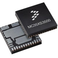
MC35XS3500PNA Freescale Semiconductor, MC35XS3500PNA Datasheet - Page 27

MC35XS3500PNA
Manufacturer Part Number
MC35XS3500PNA
Description
IC SWITCH HIGHSIDE 24PQFN
Manufacturer
Freescale Semiconductor
Type
High Side Switchr
Datasheet
1.MC35XS3500PNAR2.pdf
(41 pages)
Specifications of MC35XS3500PNA
Number Of Outputs
5
Rds (on)
*
Internal Switch(s)
Yes
Current Limit
9A
Voltage - Input
7 V ~ 20 V
Operating Temperature
-40°C ~ 125°C
Mounting Type
Surface Mount
Package / Case
24-PQFN, 24-PowerQFN
Product
MOSFET Gate Drivers
Rise Time
50 ns
Fall Time
50 ns
Propagation Delay Time
6.5 ms
Supply Voltage (max)
+ 5.5 V
Supply Voltage (min)
- 0.3 V
Supply Current
20 mA
Maximum Operating Temperature
+ 125
Minimum Operating Temperature
- 40 C
Lead Free Status / RoHS Status
Lead free / RoHS Compliant
Available stocks
Company
Part Number
Manufacturer
Quantity
Price
period.
ADDRESS 01010 — Control OUT2
ADDRESS 011111 — Control OUT3
ADDRESS 01100 — Control OUT4
ADDRESS 01101 — Control OUT5
ADDRESS 01110 — Control External Switch
ADDRESS 01111 — Test Mode
the SPI during normal operation.
Serial Output Communication (Device Status
Return
Data)
loaded. Meanwhile, the data clocks out the MSB first as the
new message data is clocked into the SI pin. The first 16 bits
of data clocking out of the SO, and following a CS transition,
Analog Integrated Circuit Device Data
Freescale Semiconductor
Overload
Status /
Device
Output
Output
Status
Status
Status
Status
Mode
Reset
D7 = 1, D6 : D0 = 00 output ON during 1/128.
D7 = 1, D6 : D0 = 1 A output ON during 27/128 on PWM
D7 = 1, D6 : D0 = 7 F output continuous ON (no PWM).
Same description as OUT1.
Same description as OUT1.
Same description as OUT1.
Same description as OUT1.
Same description as OUT1.
This register is reserved for test and is not available with
When the CS pin is pulled low, the output register is
Previous
SO
A1
SI Data
X
0
0
1
1
SO
A0
X
0
1
0
1
OD1
5
0
0
1
1
0
OD1
4
0
1
0
1
0
OD13 OD12 OD11
UVF OTW OTS
UVF OTW OTS
UVF OTW OTS
UVF OTW OTS
0
0
Table 11. Serial Output Bit Map Description
0
OD1
NM
NM
NM
NM
0
1
OD9
OC5 OTS5 OC4 OTS4 OC3 OTS3
OL5
0
0
0
OVL5
OD8
OV
0
0
is dependant upon the previously written SPI word (SOA1
and SOA0 defined in the last SPI initialization word).
representative of the initial message bits clocked into the SI
pin, since the CS pin first transitioned to a logic [0]. This
feature is useful for daisy chaining devices.
transition of logic [0] to logic [1]. If the message length is
valid, the data is latched into the appropriate registers. A valid
message length is a multiple of 16 bits. At this time, the SO
pin is tri-stated and the fault status register is now able to
accept new fault status information.
the Initialization-selected register data at the time that the CS
is pulled to a logic [0] during SPI communication and / or for
the period of time since the last valid SPI communication,
with the following exceptions:
Serial Output Bit Assignment
from the most recent initialization command SOA[1:0] (refer
to
follow.
the fault is removed.
reflects Normal mode (NM).
SO Data
STOP
Table
Any bits clocked out of the SO pin after the first 16 will be
A valid message length is determined following a CS
The output status register correctly reflects the status of
• The previous SPI communication was determined to be
• Battery transients below 6.0V, resulting in an under-
The contents of bits OD15 : OD0 depend on bits D1: D0
The register bits are reset by a read operation and also if
Table 11
OD7
_ON
OL4
X
0
invalid. In this case, the status will be reported as
though the invalid SPI communication never occurred.
voltage shutdown of the outputs, may result in incorrect
data loaded into the SPI register, except the UVF fault
reporting (OD13).
8, page 25), as explained in the paragraphs that
HER_
OVL4
FLAS
OD6
ON
X
0
summarizes the SO register content. Bit OD10
IGN_
OD5
OL3
ON
X
0
OVL3
OUT5
OD4
RC
LOGIC COMMANDS AND REGISTERS
0
FUNCTIONAL DEVICE OPERATION
STOP
OUT4
OD3
OC2
OL2
pin
0
FLASHER
OTS2
OVL2
OUT3
OD2
pin
0
OUT2
OD1
OC1 OTS1
OL1
IGN
pin
0
35XS3500
CLOCK
OVL1
OUT1
OD0
fail
0
27


