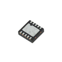
SP6652ER-L Exar Corporation, SP6652ER-L Datasheet - Page 5

SP6652ER-L
Manufacturer Part Number
SP6652ER-L
Description
IC PWM BUCK CURRENT MODE 10DFN
Manufacturer
Exar Corporation
Type
Step-Down (Buck)r
Datasheet
1.SP6652ER-L.pdf
(16 pages)
Specifications of SP6652ER-L
Package / Case
10-VFDFN Exposed Pad
Internal Switch(s)
Yes
Synchronous Rectifier
Yes
Number Of Outputs
1
Voltage - Output
0.9 V ~ 5 V
Current - Output
1A
Frequency - Switching
1.4MHz
Voltage - Input
2.85 V ~ 5.5 V
Operating Temperature
-40°C ~ 85°C
Mounting Type
*
Output Voltage
Adjustable
Output Current
1 A
Input Voltage
2.85 V to 5.5 V
Mounting Style
SMD/SMT
Duty Cycle (max)
100 %
Lead Free Status / RoHS Status
Lead free / RoHS Compliant
Lead Free Status / RoHS Status
Lead free / RoHS Compliant, Lead free / RoHS Compliant
Other names
1016-1216
Available stocks
Company
Part Number
Manufacturer
Quantity
Price
Company:
Part Number:
SP6652ER-L/TR
Manufacturer:
EXAR
Quantity:
2 000
Current Mode Control and Slope
Compensation
The SP6652 is designed to use low value
ceramic capacitors and low value inductors
to reduce the converter’s volume and cost
in portable devices. Current mode PWM
control was, therefore, chosen for the ease
of compensation when using ceramic output
capacitors and better transient line rejec-
tion, which is important in battery powered
applications. Current mode control spreads
the two poles of the output power train filter
far apart so that the modulator gain crosses
over at -20dB/decade instead of the usual
-40dB/decade. The external compensation
network is, simply, a series RC circuit con-
nected between ground and the output of the
internal transconductance error amplifier.
It is well known that an unconditional insta-
bility exists for any fixed frequency current-
mode converter operating above 50% duty
cycle. A simple, constant-slope compensa-
tion is chosen to achieve stability under these
conditions. The most common high duty
cycle application is a Li-Ion battery powered
regulator with a 3.3V output (D ≥ 90%). Since
the current loop is critically damped when the
compensation slope (denoted MC
the negative discharge slope (denoted M2
the amount of slope compensation chosen
is, therefore:
M2 = dI
M2
MC
for R
The inductor current is sensed as a voltage
across the PMOS charging switch and the
NMOS synchronous rectifier (see BLOCK
DIAGRAM). During inductor current charge,
V(PV
Oct10-07 RevJ
-702mA/µs
V
V
= M2•R
PMOS
= -M2
IN
)-V(LX) represents the charging cur-
L
/dT
= 0.20Ω
V
= 702mA/µs•0.2Ω = 140mV/µs,
OFF
PMOS
=-V
OUT
SP6652 1A, High Efficiency, Current Mode PWM Buck Regulator
/L = -3.3V/4.7µH =
V
) equals
V
),
5
rent ramp times the resistance of the PMOS
charging switch. To keep the effective current
slope compensation constant (remembering
current is being compensated, not voltage)
the voltage slope must be proportional to
R
pensation voltage is internally generated
with a bias current that is also proportional
to R
Over Current Protection
In steady state closed loop operation the
voltage at the COMP pin controls the duty
cycle. Due to the current mode control and the
slope compensation, this voltage will be:
V(
The COMP node will be clamped when its
voltage tries to exceed V(
The V
at the output of the translator. The correct
value of clamp voltage is, therefore:
V(
The I
current that is proportional to R
keep the value of current limit approximately
constant over process and temperature
variations, while the MC
by a peak-holding circuit that senses the
amplitude of the slope compensation ramp
at the end of T
There is minimum on-time (T
even if the COMP node is at zeroV, since
the peak current comparator is reset at the
end of a charge cycle and is held low during
a blanking time after the start of the next
charge cycle. This is necessary to swamp
the transients in the inductor current ramp
around switching times. The minimum T
(100ns, nominally) is not sufficient for the
COMP node to keep control of the current
PMOS
COMP
BLIM
PMOS
L(MAX)
) = I
BE
. To account for this, the slope com-
)•
(Q1) term is cancelled by V
{
.
I
L
LPK
(
MAX
term is generated with a bias
•R
ON
)• R
DetaileD Description
PMOS
.
PMOS
+ MC
V
+ MCV •T
•T
V
© 2007 Sipex Corporation
BLIM
•T
ON
ON
ON
) + V
is generated
) generated
+ V
ON
PMOS
BE
BE
BE
(Q1)
(Q1).
(Q2)
, to
ON
}


