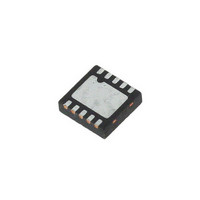
SP6652ER-L Exar Corporation, SP6652ER-L Datasheet - Page 8

SP6652ER-L
Manufacturer Part Number
SP6652ER-L
Description
IC PWM BUCK CURRENT MODE 10DFN
Manufacturer
Exar Corporation
Type
Step-Down (Buck)r
Datasheet
1.SP6652ER-L.pdf
(16 pages)
Specifications of SP6652ER-L
Package / Case
10-VFDFN Exposed Pad
Internal Switch(s)
Yes
Synchronous Rectifier
Yes
Number Of Outputs
1
Voltage - Output
0.9 V ~ 5 V
Current - Output
1A
Frequency - Switching
1.4MHz
Voltage - Input
2.85 V ~ 5.5 V
Operating Temperature
-40°C ~ 85°C
Mounting Type
*
Output Voltage
Adjustable
Output Current
1 A
Input Voltage
2.85 V to 5.5 V
Mounting Style
SMD/SMT
Duty Cycle (max)
100 %
Lead Free Status / RoHS Status
Lead free / RoHS Compliant
Lead Free Status / RoHS Status
Lead free / RoHS Compliant, Lead free / RoHS Compliant
Other names
1016-1216
Available stocks
Company
Part Number
Manufacturer
Quantity
Price
Company:
Part Number:
SP6652ER-L/TR
Manufacturer:
EXAR
Quantity:
2 000
Complete Application Circuit.
Oct10-07 RevJ
The SP6652 PWM buck regulator circuit
requires 3 capacitors: 10µF for the P
1µF input bypass for the S
for the output are typically recommended.
For the input capacitor, a value even larger
than 10µF will help reduce input voltage
ripple for applications sensitive to ripple on
the battery voltage. See the Typical Per-
formance Characteristics section for wave-
forms on input and output ripple with 10µF
capacitors. All the capacitors should be
surface mount ceramic for low lead induc-
tance necessary at the 1.4MHz switching
frequency of the SP6652 and to obtain low
ESR. This also helps improve bypassing
on the input pin and ripple on the output.
Ceramic capacitors with X5R or X7R tem-
perature grade are recommended for most
applications. A selection of recommended
capacitors is included in Table 1. The 1µF
S
resistor of about 10Ω value connected
from the input to the S
low pass filter to remove high frequency
spikes present on the input switching pin
COMPONENT SELECTION
VIN
input capacitor should have a series
VOUT
10µF
C3
R
R
FBH
FBL
VIN
SP6652 1A, High Efficiency, Current Mode PWM Buck Regulator
pin to form an RC
VIN
SYNC
10nF
4kΩ
Cc
Rz
V
and 10µF
SD
IN
VIN
4.7µH
input,
L1
1
2
3
4
5
PGND
SGND
FB
COMP
SD
SP6652
8
MODE
P
reference and other sensitive circuits noise
free and ensure better output regulation.
The GND returns for the P
the output capacitor should be connected
directly to the P
nect to the thermal pad ground located un-
der the SP6652. The GND return for the
1µF S
the S
separately to the P
P
the Typical SP6652 Circuit Layout for de-
tails on the recommended layout.
Output Voltage Selection
To set the output voltage for the SP6652,
a pair of resistors, R
voltage divider between the output voltage
at the output capacitor and the FB pin and
GND, as shown in the typical application cir-
cuit. The recommended value for the R
sistor is 100KΩ to 200KΩ to keep the quies-
cent current low, but not have the impedance
too high at the FB pin for good regulation.
SYNC
PVIN
SVIN
VIN
GND
LX
.
GND
noise to the SP6652 S
10
9
8
7
6
VIN
This will keep the SP6652 internal
APPLICATIONS INFORMATION
capacitor should be connected to
pin, which should be connected
1µF
C2
GND
10Ω
R1
GND
pin, which should con-
F
and R
pin to avoid adding
10µF
© 2007 Sipex Corporation
VIN
C1
I
VIN
are used as a
capacitor and
GND
pin. See
I
re-


