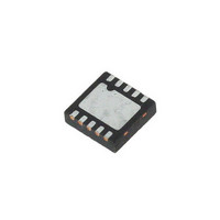
SP6652ER-L Exar Corporation, SP6652ER-L Datasheet - Page 6

SP6652ER-L
Manufacturer Part Number
SP6652ER-L
Description
IC PWM BUCK CURRENT MODE 10DFN
Manufacturer
Exar Corporation
Type
Step-Down (Buck)r
Datasheet
1.SP6652ER-L.pdf
(16 pages)
Specifications of SP6652ER-L
Package / Case
10-VFDFN Exposed Pad
Internal Switch(s)
Yes
Synchronous Rectifier
Yes
Number Of Outputs
1
Voltage - Output
0.9 V ~ 5 V
Current - Output
1A
Frequency - Switching
1.4MHz
Voltage - Input
2.85 V ~ 5.5 V
Operating Temperature
-40°C ~ 85°C
Mounting Type
*
Output Voltage
Adjustable
Output Current
1 A
Input Voltage
2.85 V to 5.5 V
Mounting Style
SMD/SMT
Duty Cycle (max)
100 %
Lead Free Status / RoHS Status
Lead free / RoHS Compliant
Lead Free Status / RoHS Status
Lead free / RoHS Compliant, Lead free / RoHS Compliant
Other names
1016-1216
Available stocks
Company
Part Number
Manufacturer
Quantity
Price
Company:
Part Number:
SP6652ER-L/TR
Manufacturer:
EXAR
Quantity:
2 000
when the output voltage is low. The inductor
current tends to rise until the energy loss
from the discharge resistances are equal to
the energy gained during the charge phase.
For this reason, the clock frequency is cut in
half when the feedback pin is below 0.3V, ef-
fectively reducing the minimum duty cycle in
half. Above V(
is normal (see Typical Operating Character-
istics: Inductor Current vs. V
Voltage Loop and Compensation
in PWM Mode
The voltage loop section of the circuit con-
sists of the error amplifier and the translator
circuits (see functional diagram). The input
of the voltage loop is the 0.8V reference volt-
age minus the divided down output voltage
at the feedback pin. The output of the error
amplifier is translated from a ground referred
signal (the COMP node) to a power input
voltage referred signal. The output of the
voltage loop is fed to the positive terminal
of the Current Loop comparator, and repre-
sents the peak inductor current necessary
to close the loop.
Oct10-07 RevJ
Linearized Modulator Frequency Response vs. Inductor
Conditions: V
1
16K
20K
12K
8K
4K
0
2
0.8M
0.4M
2.0M
1.6M
1.2M
2µH to 10µH
FB
0
IN
) = 0.3V the clock frequency
=5V, V
3
40K
20K
30K
10K
50K
>>
0
2u
1
OUT
Mod_pole1
SP6652 1A, High Efficiency, Current Mode PWM Buck Regulator
=3.3V, f
OUT
3u
CLK
2
)
=1.4MHz, C
Mod_pole2
4u
OUT
3
6
=10µF, and MC
5u
Gbw_modfb
The total power supply loop is compensated
with a series RC network connected from
the COMP pin to ground. Compensation is
simple due to current-mode control. The
modulator has two dominant poles: one at a
low frequency, and one above the crossover
frequency of the loop, as seen in the graph
below, Linearized Modulator Frequency
Response vs. Inductor Value.
The low frequency pole for L1= 5µH is
4kHz, the second pole is 500kHz, and the
gain-bandwidth is 20kHz. The total loop
crossover frequency is chosen to be 200kHz,
which is 1/6
sets the second modulator pole at 2.5 times
the crossover frequency. Therefore the gain
of the error amplifier can be 200kHz/20kHz
= 10 at the first modulator pole of 4kHz. The
error amp transconductance is 1mA/V, so
this sets the R
pensation network at 10/1mA/V = 10kΩ.
The zero frequency is placed at the first
pole to provide at total system response of
-20dB/decade (the zero from the error amp
cancels the first modulator pole, leaving the
L1VAL
6u
V
=132mV/µs. The inductor is varied from
th
7u
of the clock frequency. This
Z
DetaileD Description
resistor value in the com-
8u
© 2007 Sipex Corporation
9u
10u


