EVL90WADP-LLCSR STMicroelectronics, EVL90WADP-LLCSR Datasheet - Page 30
EVL90WADP-LLCSR
Manufacturer Part Number
EVL90WADP-LLCSR
Description
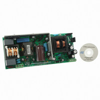
EVAL BOARD PORTABLE PWR SUPPLY
Manufacturer
STMicroelectronics
Type
Power Factor Correctionr
Datasheets
1.L6563HTR.pdf
(49 pages)
2.L6599ADTR.pdf
(36 pages)
3.EVL90WADP-LLCSR.pdf
(29 pages)
4.EVL90WADP-LLCSR.pdf
(28 pages)
Specifications of EVL90WADP-LLCSR
Main Purpose
AC/DC, Primary and Secondary Side with PFC
Outputs And Type
1, Isolated
Power - Output
90W
Voltage - Output
19V
Current - Output
4.75A
Voltage - Input
90 ~ 264VAC
Regulator Topology
Boost
Frequency - Switching
130kHz
Board Type
Fully Populated
Utilized Ic / Part
L6563H, L6599A, SRK2000
Input Voltage
90 V to 264 V
Output Voltage
19 V
Dimensions
65 mm x 155 mm
Product
Power Management Modules
Supply Current
4.75 A
Lead Free Status / RoHS Status
Lead free / RoHS Compliant
For Use With/related Products
L6563H, L6599A, SRK2000
Other names
497-10377


Application information
30/49
V(TBO)/RT, that is internally 1:1 mirrored and sunk from pin INV (#1) input of the L6563H's
error amplifier. In this way, when the mains voltage increases the voltage at TBO pin
increases as well and so does the current flowing through the resistor connected between
TBO and GND. Then a larger current is sunk by INV pin and the output voltage of the PFC
pre-regulator is forced to get higher. Obviously, the output voltage moves in the opposite
direction if the input voltage decreases.
To avoid undesired output voltage rise should the mains voltage exceed the maximum
specified value, the voltage at the TBO pin is clamped at 3V. By properly selecting the
multiplier bias it is possible to set the maximum input voltage above which input-to-output
tracking ends and the output voltage becomes constant. If this function is not used, leave
the pin open: the device regulates a fixed output voltage.
Starting from the following data:
●
●
●
●
●
to set the output voltage at the desired values use the following design procedure:
1.
2.
3.
4.
5.
Figure 43
Vin
Vin
Vo
Vo
Vox = absolute maximum limit for the regulated output voltage;
Determine the input RMS voltage Vinclamp that produces Vo = Vox:
and choose a value Vin
the output voltage range below Vox (it is equal Vox if one chooses Vin
Determine the divider ratio of the MULT pin (#3) bias:
and check that at minimum mains voltage Vin1 the peak voltage on pin 3 is greater than
0.65 V.
Determine R1, the upper resistor of the output divider, for instance 3 MΩ.
Calculate the lower resistor R2 of the output divider and the adjustment resistor RT:
Check that the maximum current sourced by the TBO pin (#6) does not exceed the
maximum specified (0.2 mA):
1
2
1
2
= regulated output voltage @ Vin = Vin
= regulated output voltage @ Vin = Vin
= minimum specified input RMS voltage;
= maximum specified input RMS voltage;
shows the internal block diagram of the tracking boost function.
⎧
⎪ ⎪
⎨
⎪
⎪
⎩
R
R
Vin
2
T
=
=
clamp
2
x
5 .
2
such that Vin
Doc ID 16047 Rev 3
⋅
⋅
=
R
k
1
⋅
I
Vox
Vo
TBO
R
⋅
(
1
Vo
2
⋅
max
Vin
−
−
Vo
1
k
Vo
Vo
−
=
2
2
=
2
2
1
1
−
−
5 .
R
≤
3
⋅
2
Vin
Vo
T
)
Vin
Vinx < Vinclamp. This results in a limitation of
⋅
⋅
3
Vin
≤
Vin
Vin
1
1
2
1
2
;
;
0
2 .
−
2
x
2
−
Vox
−
Vo
⋅
10
(
Vin
Vo
2
−
−
3
−
1
2
Vo
Vo
−
2
2
1
5 .
⋅
)
Vin
⋅
Vin
1
1
x
= Vin
clamp
L6563H
)
Related parts for EVL90WADP-LLCSR
Image
Part Number
Description
Manufacturer
Datasheet
Request
R

Part Number:
Description:
STMicroelectronics [RIPPLE-CARRY BINARY COUNTER/DIVIDERS]
Manufacturer:
STMicroelectronics
Datasheet:
Part Number:
Description:
STMicroelectronics [LIQUID-CRYSTAL DISPLAY DRIVERS]
Manufacturer:
STMicroelectronics
Datasheet:

Part Number:
Description:
BOARD EVAL FOR MEMS SENSORS
Manufacturer:
STMicroelectronics
Datasheet:
Part Number:
Description:
NPN TRANSISTOR POWER MODULE
Manufacturer:
STMicroelectronics
Datasheet:
Part Number:
Description:
TURBOSWITCH ULTRA-FAST HIGH VOLTAGE DIODE
Manufacturer:
STMicroelectronics
Datasheet:
Part Number:
Description:
Manufacturer:
STMicroelectronics
Datasheet:
Part Number:
Description:
DIODE / SCR MODULE
Manufacturer:
STMicroelectronics
Datasheet:
Part Number:
Description:
DIODE / SCR MODULE
Manufacturer:
STMicroelectronics
Datasheet:
Part Number:
Description:
Search -----> STE16N100
Manufacturer:
STMicroelectronics
Datasheet:
Part Number:
Description:
Search ---> STE53NA50
Manufacturer:
STMicroelectronics
Datasheet:
Part Number:
Description:
NPN Transistor Power Module
Manufacturer:
STMicroelectronics
Datasheet:
Part Number:
Description:
DIODE / SCR MODULE
Manufacturer:
STMicroelectronics
Datasheet: