EVL90WADP-LLCSR STMicroelectronics, EVL90WADP-LLCSR Datasheet - Page 8
EVL90WADP-LLCSR
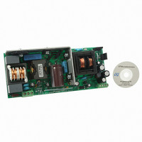
Manufacturer Part Number
EVL90WADP-LLCSR
Description
EVAL BOARD PORTABLE PWR SUPPLY
Manufacturer
STMicroelectronics
Type
Power Factor Correctionr
Datasheets
1.L6563HTR.pdf
(49 pages)
2.L6599ADTR.pdf
(36 pages)
3.EVL90WADP-LLCSR.pdf
(29 pages)
4.EVL90WADP-LLCSR.pdf
(28 pages)
Specifications of EVL90WADP-LLCSR
Main Purpose
AC/DC, Primary and Secondary Side with PFC
Outputs And Type
1, Isolated
Power - Output
90W
Voltage - Output
19V
Current - Output
4.75A
Voltage - Input
90 ~ 264VAC
Regulator Topology
Boost
Frequency - Switching
130kHz
Board Type
Fully Populated
Utilized Ic / Part
L6563H, L6599A, SRK2000
Input Voltage
90 V to 264 V
Output Voltage
19 V
Dimensions
65 mm x 155 mm
Product
Power Management Modules
Supply Current
4.75 A
Lead Free Status / RoHS Status
Lead free / RoHS Compliant
For Use With/related Products
L6563H, L6599A, SRK2000
Other names
497-10377


Pin connection
3
Table 3.
8/49
n°
1
2
3
4
5
6
COMP
Name
MULT
TBO
VFF
INV
CS
Pin connection
Figure 2.
Pin description
Inverting input of the error amplifier. The information on the output voltage of the PFC pre-
regulator is fed into the pin through a resistor divider.
The pin normally features high impedance but, if the tracking boost function is used, an internal
current generator programmed by TBO (pin 6) is activated. It sinks current from the pin to
change the output voltage so that it tracks the mains voltage.
Output of the error amplifier. A compensation network is placed between this pin and INV (pin
1) to achieve stability of the voltage control loop and ensure high power factor and low THD.
To avoid uncontrolled rise of the output voltage at zero load, when the voltage on the pin falls
below 2.4 V the gate driver output is inhibited (burst-mode operation).
Mains input to the multiplier. This pin is connected to the rectified mains voltage via a resistor
divider and provides the sinusoidal reference to the current loop. The voltage on this pin is used
also to derive the information on the RMS mains voltage.
Input to the PWM comparator. The current flowing in the MOSFET is sensed through a resistor,
the resulting voltage is applied to this pin and compared with an internal reference to determine
MOSFET’s turn-off.
A second comparison level at 1.7 V detects abnormal currents (e.g. due to boost inductor
saturation) and, on this occurrence, activates a safety procedure that temporarily stops the
converter and limits the stress of the power components.
Second input to the multiplier for 1/V
connected from the pin to GND. They complete the internal peak-holding circuit that derives the
information on the RMS mains voltage. The voltage at this pin, a dc level equal to the peak
voltage on pin MULT (3), compensates the control loop gain dependence on the mains voltage.
Never connect the pin directly to GND but with a resistor ranging from 100 kΩ (minimum) to 2 M
Ω (maximum).
Tracking boost function. This pin provides a buffered VFF voltage. A resistor connected
between this pin and GND defines a current that is sunk from pin INV (1). In this way, the output
voltage is changed proportionally to the mains voltage (tracking boost). If this function is not
used leave this pin open.
Pin connection
Doc ID 16047 Rev 3
2
function. A capacitor and a parallel resistor must be
Function
L6563H
Related parts for EVL90WADP-LLCSR
Image
Part Number
Description
Manufacturer
Datasheet
Request
R

Part Number:
Description:
STMicroelectronics [RIPPLE-CARRY BINARY COUNTER/DIVIDERS]
Manufacturer:
STMicroelectronics
Datasheet:
Part Number:
Description:
STMicroelectronics [LIQUID-CRYSTAL DISPLAY DRIVERS]
Manufacturer:
STMicroelectronics
Datasheet:

Part Number:
Description:
BOARD EVAL FOR MEMS SENSORS
Manufacturer:
STMicroelectronics
Datasheet:
Part Number:
Description:
NPN TRANSISTOR POWER MODULE
Manufacturer:
STMicroelectronics
Datasheet:
Part Number:
Description:
TURBOSWITCH ULTRA-FAST HIGH VOLTAGE DIODE
Manufacturer:
STMicroelectronics
Datasheet:
Part Number:
Description:
Manufacturer:
STMicroelectronics
Datasheet:
Part Number:
Description:
DIODE / SCR MODULE
Manufacturer:
STMicroelectronics
Datasheet:
Part Number:
Description:
DIODE / SCR MODULE
Manufacturer:
STMicroelectronics
Datasheet:
Part Number:
Description:
Search -----> STE16N100
Manufacturer:
STMicroelectronics
Datasheet:
Part Number:
Description:
Search ---> STE53NA50
Manufacturer:
STMicroelectronics
Datasheet:
Part Number:
Description:
NPN Transistor Power Module
Manufacturer:
STMicroelectronics
Datasheet:
Part Number:
Description:
DIODE / SCR MODULE
Manufacturer:
STMicroelectronics
Datasheet: