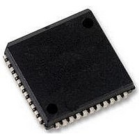
SC28L92A1A NXP Semiconductors, SC28L92A1A Datasheet - Page 55

SC28L92A1A
Manufacturer Part Number
SC28L92A1A
Description
UART, DUAL, 3.3V OR 5V, SMD, 28L92
Manufacturer
NXP Semiconductors
Datasheet
1.SC28L92A1B557.pdf
(73 pages)
Specifications of SC28L92A1A
No. Of Channels
2
Supply Voltage Range
2.97V To 3.63V, 4.5V To 5.5V
Operating Temperature Range
-40°C To +85°C
Digital Ic Case Style
PLCC
No. Of Pins
44
Svhc
No SVHC (18-Jun-2010)
Operating
RoHS Compliant
Data Rate
230.4Kilobaud
Uart Features
Programmable Channel Mode, Line Break Detection & Generation
Rohs Compliant
Yes
Available stocks
Company
Part Number
Manufacturer
Quantity
Price
Company:
Part Number:
SC28L92A1A
Manufacturer:
NXP
Quantity:
677
Company:
Part Number:
SC28L92A1A,512
Manufacturer:
NXP Semiconductors
Quantity:
10 000
Company:
Part Number:
SC28L92A1A,518
Manufacturer:
NXP Semiconductors
Quantity:
10 000
Company:
Part Number:
SC28L92A1A,529
Manufacturer:
NXP Semiconductors
Quantity:
10 000
Company:
Part Number:
SC28L92A1A529
Manufacturer:
NXP Semiconductors
Quantity:
135
NXP Semiconductors
Table 67.
V
[1]
[2]
[3]
[4]
[5]
[6]
SC28L92_7
Product data sheet
Symbol
Clock timing (see
t
f
t
f
t
f
t
f
Transmitter timing, external clock (see
t
t
Receiver timing, external clock (see
t
t
68xxx or Motorola bus timing (see
t
t
t
t
CLK
CLK
CTC
CTC
RX
RX
TX
TX
TXD
TCS
RXS
RXH
DCR
DCW
DAT
CSC
CC
= 5.0 V
The following conditions apply:
a) Parameters are valid over specified temperature and voltage range.
b) All voltage measurements are referenced to ground. For testing, all inputs swing between 0.4 V and 3.0 V with a transition time of
c) Test conditions for outputs: C
d) Typical values are the average values at +25 C and 5 V.
Timing is illustrated and referenced to the WRN and RDN Inputs. Also, CEN may be the strobing input. CEN and RDN (also CEN and
WRN) are ORed internally. The signal asserted last initiates the cycle and the signal negated first terminates the cycle.
Guaranteed by characterization of sample units.
If CEN is used as the strobing input, the parameter defines the minimum HIGH times between one CEN and the next. The RDN signal
must be negated for t
Minimum frequencies are not tested but are guaranteed by design.
Clocks for 1 mode should maintain a 60/40 duty cycle or better.
5 ns maximum. For X1/CLK this swing is between 0.4 V and 0.8V
and 2.0 V, and output voltages of 0.8 V and 2.0 V, as appropriate.
constant current source = 2.6 mA.
Parameter
X1/CLK HIGH or LOW time
X1/CLK frequency
C/T clock (IP2) HIGH or LOW time (C/T
external clock input)
C/T clock (IP2) frequency
RxC HIGH or LOW time
RxC frequency
TxC HIGH or LOW time
TxC frequency
TxD output delay from TxC LOW (TxC
input pin)
output delay from TxC output pin LOW to
TxD data output
RxD data set-up time to RxC HIGH
RxD data hold time from RxC HIGH
DACKN LOW (read cycle) from X1 HIGH
DACKN LOW (write cycle) from X1 HIGH
DACKN high-impedance from CEN or
IACKN HIGH
CEN or IACKN set-up time to X1 HIGH for
minimum DACKN cycle
Dynamic characteristics, 5 V operation
10 %, T
Figure
amb
RWD
= 40 C to +85 C, unless otherwise specified.
17)
to guarantee that any status register changes are valid.
L
= 125 pF, except open-drain outputs. Test conditions for open-drain outputs: C
Figure
Figure
Figure
12,
19)
Rev. 07 — 19 December 2007
13
18)
3.3 V/5.0 V Dual Universal Asynchronous Receiver/Transmitter
and 14)
[1]
Conditions
16
16
1
16
16
1
…continued
[7]
CC
. All time measurements are referenced at input voltages of 0.8 V
[5][6]
[5][6]
[5]
[5]
[7]
Min
30
0.1
30
0
30
0
0
30
-
0
-
-
50
50
-
-
-
16
Typ
20
3.686
10
-
10
-
-
10
-
-
40
6
40
40
15
15
8
8
SC28L92
© NXP B.V. 2007. All rights reserved.
L
= 125 pF,
Max
-
8
-
8
-
16
1
-
16
1
60
30
-
-
35
35
10
-
55 of 73
Unit
ns
MHz
ns
MHz
ns
MHz
MHz
ns
MHz
MHz
ns
ns
ns
ns
ns
ns
ns
ns


