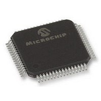
DSPIC30F5011-30I/PTG Microchip Technology, DSPIC30F5011-30I/PTG Datasheet - Page 133

DSPIC30F5011-30I/PTG
Manufacturer Part Number
DSPIC30F5011-30I/PTG
Description
16BIT MCU-DSP 30MHZ, SMD, 30F5011
Manufacturer
Microchip Technology
Series
DsPIC30Fr
Datasheet
1.DSPIC30F5011-30IPTG.pdf
(220 pages)
Specifications of DSPIC30F5011-30I/PTG
Core Frequency
30MHz
Embedded Interface Type
CAN, I2C, SPI, UART
No. Of I/o's
52
Flash Memory Size
66KB
Supply Voltage Range
2.5V To 5.5V
Operating Temperature Range
-40°C To
Lead Free Status / RoHS Status
Lead free / RoHS Compliant
- Current page: 133 of 220
- Download datasheet (4Mb)
19.8
The module has 2 internal Power modes.
When the ADON bit is ‘1’, the module is in Active mode;
it is fully powered and functional.
When ADON is ‘0’, the module is in Off mode. The dig-
ital and analog portions of the circuit are disabled for
maximum current savings.
In order to return to the Active mode from Off mode, the
user must wait for the ADC circuitry to stabilize.
19.9
19.9.1
When the device enters Sleep mode, all clock sources
to the module are shutdown and stay at logic ‘0’.
If Sleep occurs in the middle of a conversion, the con-
version is aborted. The converter will not continue with
a partially completed conversion on exit from Sleep
mode.
Register contents are not affected by the device
entering or leaving Sleep mode.
The A/D module can operate during Sleep mode if the
A/D clock source is set to RC (ADRC = 1). When the RC
clock source is selected, the A/D module waits one
instruction cycle before starting the conversion. This
allows the SLEEP instruction to be executed which elim-
inates all digital switching noise from the conversion.
When the conversion is complete, the CONV bit will be
cleared and the result loaded into the ADCBUF register.
FIGURE 19-3:
2004 Microchip Technology Inc.
RAM Contents:
Read to Bus:
Module Power-down Modes
A/D Operation During CPU Sleep
and Idle Modes
Signed Fractional
A/D OPERATION DURING CPU
SLEEP MODE
Signed Integer
Fractional
Integer
A/D OUTPUT DATA FORMATS
d11 d10 d09 d08 d07 d06 d05 d04 d03 d02 d01 d00
d11 d10 d09 d08 d07 d06 d05 d04 d03 d02 d01 d00
d11 d11 d11 d11 d11 d10 d09 d08 d07 d06 d05 d04 d03 d02 d01 d00
0
0
0
0
Preliminary
d11 d10 d09 d08 d07 d06 d05 d04 d03 d02 d01 d00
d11 d10 d09 d08 d07 d06 d05 d04 d03 d02 d01 d00
If the A/D interrupt is enabled, the device will wake-up
from Sleep. If the A/D interrupt is not enabled, the
D module will then be turned off, although the ADON bit
will remain set.
19.9.2
The ADSIDL bit selects if the module will stop on Idle or
continue on Idle. If ADSIDL = 0, the module will con-
tinue operation on assertion of Idle mode. If ADSIDL =
1, the module will stop on Idle.
19.10 Effects of a Reset
A device Reset forces all registers to their Reset state.
This forces the A/D module to be turned off, and any
conversion and sampling sequence is aborted. The val-
ues that are in the ADCBUF registers are not modified.
The A/D Result register will contain unknown data after
a Power-on Reset.
19.11 Output Formats
The A/D result is 12 bits wide. The data buffer RAM is
also 12 bits wide. The 12-bit data can be read in one of
four different formats. The FORM<1:0> bits select the
format. Each of the output formats translates to a 16-bit
result on the data bus. Write data will always be in right
justified (integer) format.
dsPIC30F5011/5013
A/D OPERATION DURING CPU IDLE
MODE
0
0
DS70116C-page 131
0
0
0
0
0
0
A/
Related parts for DSPIC30F5011-30I/PTG
Image
Part Number
Description
Manufacturer
Datasheet
Request
R

Part Number:
Description:
IC DSPIC MCU/DSP 66K 64TQFP
Manufacturer:
Microchip Technology
Datasheet:

Part Number:
Description:
IC,DSP,16-BIT,CMOS,TQFP,64PIN,PLASTIC
Manufacturer:
Microchip Technology
Datasheet:

Part Number:
Description:
IC DSPIC MCU/DSP 66K 64TQFP
Manufacturer:
Microchip Technology
Datasheet:

Part Number:
Description:
High-Performance Digital Signal Controllers
Manufacturer:
MICROCHIP [Microchip Technology]
Datasheet:

Part Number:
Description:
IC, DSC, 16BIT, 66KB, 40MHZ 5.5V TQFP-64
Manufacturer:
Microchip Technology
Datasheet:

Part Number:
Description:
Digital Signal Processors & Controllers - DSP, DSC 16 Bit MCU/DSP 64LD 20M 66KB FL
Manufacturer:
Microchip Technology

Part Number:
Description:
IC DSPIC MCU/DSP 66K 64TQFP
Manufacturer:
Microchip Technology
Datasheet:

Part Number:
Description:
Dspic30f5011/5013 High-performance Digital Signal Controllers
Manufacturer:
Microchip Technology Inc.
Datasheet:

Part Number:
Description:
Manufacturer:
Microchip Technology Inc.
Datasheet:

Part Number:
Description:
Manufacturer:
Microchip Technology Inc.
Datasheet:

Part Number:
Description:
Manufacturer:
Microchip Technology Inc.
Datasheet:

Part Number:
Description:
Manufacturer:
Microchip Technology Inc.
Datasheet:


