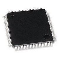
LCMXO256C-5TN100C LATTICE SEMICONDUCTOR, LCMXO256C-5TN100C Datasheet - Page 216

LCMXO256C-5TN100C
Manufacturer Part Number
LCMXO256C-5TN100C
Description
MACHXO PLD FLASH, SCRAM 1.8V, 256
Manufacturer
LATTICE SEMICONDUCTOR
Series
MachXOr
Datasheet
1.LCMXO1200C-5TN144C.pdf
(244 pages)
Specifications of LCMXO256C-5TN100C
Cpld Type
FLASH
No. Of Macrocells
128
No. Of I/o's
78
Propagation Delay
3.5ns
Global Clock Setup Time
1.3ns
Frequency
600MHz
Supply Voltage Range
1.71V To 3.465V
Operating
RoHS Compliant
Available stocks
Company
Part Number
Manufacturer
Quantity
Price
Company:
Part Number:
LCMXO256C-5TN100C
Manufacturer:
Lattice Semiconductor Corporation
Quantity:
10 000
- Current page: 216 of 244
- Download datasheet (9Mb)
Lattice Semiconductor
Implementing Multiplexers
The flexible configurations of LUTs can realize any 4-, 5-, or 6-input logic function like 2-to-1, 3-to-1 or 4-to-1 multi-
plexers. Larger multiplexers can be efficiently created by programming multiple 4-input LUTs. Synthesis tools camn
automatically infer Lattice FPGA optimized multiplexer library elements based on the behavioral description in the
HDL source code. This provides the flexibility to the Mapper and Place and Route tools to configure the LUT mode
and connections in the most optimum fashion.
Clock Dividers
There are two ways to implement clock dividers in Lattice Semiconductor FPGA devices. The first is to cascade the
registers with asynchronous clocks. The register output feeds the clock pin of the next register (Figure 13-7). Since
the clock number in each PFU is limited to two, any clock divider with more than two bits will require multiple PFU
implementations. As a result, the asynchronous daisy chaining implementation of clock divider will be slower due to
the inter-PFU routing delays. This kind of delays is usually ambiguous and inconsistent because of the nature of
FPGA routing structures.
Figure 13-7. Daisy Chaining of Flip-flops
16:1 MUX
…
process(sel, din)
…
LU
D
begin
end process;
if
elsif (sel="0001") then muxout <= din(1);
elsif (sel="0010") then muxout <= din(2);
elsif (sel="0011") then muxout <= din(3);
elsif (sel="0100") then muxout <= din(4);
elsif (sel="0101") then muxout <= din(5);
elsif (sel="0110") then muxout <= din(6);
elsif (sel="0111") then muxout <= din(7);
elsif (sel="1000") then muxout <= din(8);
elsif (sel="1001") then muxout <= din(9);
elsif (sel="1010") then muxout <= din(10);
elsif (sel="1011") then muxout <= din(11);
elsif (sel="1100") then muxout <= din(12);
elsif (sel="1101") then muxout <= din(13);
elsif (sel="1110") then muxout <= din(14);
elsif (sel="1111") then muxout <= din(15);
else muxout <= '0';
end if;
PFU
(sel="0000") then muxout <= din(0);
13-10
LU
D
PFU
HDL Synthesis Coding Guidelines
for Lattice Semiconductor FPGAs
Related parts for LCMXO256C-5TN100C
Image
Part Number
Description
Manufacturer
Datasheet
Request
R
Part Number:
Description:
IC, CPLD, FLASH, 256 MACROCELL, TQFP-100
Manufacturer:
LATTICE SEMICONDUCTOR

Part Number:
Description:
IC, CPLD, FLASH, 256 MACROCELL, TQFP-100
Manufacturer:
LATTICE SEMICONDUCTOR
Part Number:
Description:
CPLD MachXO Family 128 Macro Cells 1.8V/2.5V/3.3V 100-Pin TQFP Tray
Manufacturer:
LATTICE SEMICONDUCTOR
Datasheet:
Part Number:
Description:
ISPLSI2032-80LT44Lattice Semiconductor [In-System Programmable High Density PLD]
Manufacturer:
Lattice Semiconductor Corp.
Datasheet:
Part Number:
Description:
IC PROGRAMMED LATTICE GAL 16V8
Manufacturer:
Lattice Semiconductor Corp.
Datasheet:
Part Number:
Description:
357-036-542-201 CARDEDGE 36POS DL .156 BLK LOPRO
Manufacturer:
Lattice Semiconductor Corp.
Datasheet:
Part Number:
Description:
357-036-542-201 CARDEDGE 36POS DL .156 BLK LOPRO
Manufacturer:
Lattice Semiconductor Corp.
Datasheet:
Part Number:
Description:
357-036-542-201 CARDEDGE 36POS DL .156 BLK LOPRO
Manufacturer:
Lattice Semiconductor Corp.
Datasheet:
Part Number:
Description:
357-036-542-201 CARDEDGE 36POS DL .156 BLK LOPRO
Manufacturer:
Lattice Semiconductor Corp.
Datasheet:
Part Number:
Description:
357-036-542-201 CARDEDGE 36POS DL .156 BLK LOPRO
Manufacturer:
Lattice Semiconductor Corp.
Datasheet:
Part Number:
Description:
357-036-542-201 CARDEDGE 36POS DL .156 BLK LOPRO
Manufacturer:
Lattice Semiconductor Corp.
Datasheet:
Part Number:
Description:
357-036-542-201 CARDEDGE 36POS DL .156 BLK LOPRO
Manufacturer:
Lattice Semiconductor Corp.
Datasheet:
Part Number:
Description:
357-036-542-201 CARDEDGE 36POS DL .156 BLK LOPRO
Manufacturer:
Lattice Semiconductor Corp.
Datasheet:
Part Number:
Description:
357-036-542-201 CARDEDGE 36POS DL .156 BLK LOPRO
Manufacturer:
Lattice Semiconductor Corp.
Datasheet:
Part Number:
Description:
357-036-542-201 CARDEDGE 36POS DL .156 BLK LOPRO
Manufacturer:
Lattice Semiconductor Corp.
Datasheet:


