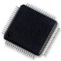
MB91F669PMC-G-JNE1 Fujitsu, MB91F669PMC-G-JNE1 Datasheet - Page 11

MB91F669PMC-G-JNE1
Manufacturer Part Number
MB91F669PMC-G-JNE1
Description
MCU, 32BIT, FR80, 128K FLASH, 64LQFP
Manufacturer
Fujitsu
Datasheet
1.MB91F668PMC-G-JNE1.pdf
(104 pages)
Specifications of MB91F669PMC-G-JNE1
No. Of I/o's
50
Ram Memory Size
16KB
Cpu Speed
33MHz
No. Of Timers
1
No. Of Pwm Channels
4
Digital Ic Case
RoHS Compliant
Core Size
32bit
Program Memory Size
128KB
Oscillator Type
Internal, External
Controller Family/series
MB91665
Rohs Compliant
Yes
- Current page: 11 of 104
- Download datasheet (4Mb)
DS07-16916-2E
64 pin 48 pin
Pin Number
24
25
26
27
28
29
30
31
32
33
34
35
16
17
18
19
20
21
22
23
24
25
26
27
INIT
PK1
X0A
PK0
X1A
C
MD1
MD0
X0
X1
V
V
P02
D02
TIOA1
SCK0_1
(SCL0_1)
IN2
P03
D03
TIOB1
IN3
SS
CC
Pin Name
Circuit
Type*
I/O
Q
P
P
P
A
A
B
I
I
*2
1
External reset input pin. A reset is valid when
INIT L.
The I/O circuit type for the flash memory
products is P.
General-purpose I/O port
Sub clock (oscillation) input pin
General-purpose I/O port
Sub clock (oscillation) I/O pin
Power stabilization capacity pin
Mode 1 pin. Input must always be at the “L”
level.
The I/O circuit type for the flash memory
products is P.
Mode 0 pin.
The I/O circuit type for the flash memory
products is P.
During normal operation, MD0 L must be
input. During serial programming to flash
memory, MD0 H must be input.
Main clock (oscillation) input pin
Main clock (oscillation) I/O pin
GND pin
Power pin
General-purpose I/O port
External bus interface data bus bit2
Base timer ch.1 TIOA pin
Multifunction serial interface ch.0 clock I/O pin
(Port 1).
This pin operates as SCK0_1 when it is used in
a UART/CSIO (operation modes 0 to 2) and as
SCL0_1 when it is used in an I
mode 4).
32-bit input capture ch.2 input pin
General-purpose I/O port
External bus interface data bus bit3
Base timer ch.1 TIOB pin
32-bit input capture ch.3 input pin
Function
2
C (operation
MB91665 Series
CMOS
input
level
hysteresis
(Continued)
CMOS
input
level
11
Related parts for MB91F669PMC-G-JNE1
Image
Part Number
Description
Manufacturer
Datasheet
Request
R

Part Number:
Description:
Fujitsu Media Devices Limited [NMOS 1- CHANNEL, 13-BIT AND 3-CHANNEL, 6-BIT D/A CONVERTER]
Manufacturer:
Fujitsu
Datasheet:

Part Number:
Description:
Fujitsu Media Devices Limited [32-bit RISC Microcontroller]
Manufacturer:
Fujitsu
Datasheet:

Part Number:
Description:
Fujitsu Media Devices Limited [MOS 262,144 BIT DYNAMIC RANDOM ACCESS MEMORY]
Manufacturer:
Fujitsu
Datasheet:

Part Number:
Description:
Fujitsu Media Devices Limited [PROGRAMMABLE TIMER]
Manufacturer:
Fujitsu
Datasheet:

Part Number:
Description:
Fujitsu Media Devices Limited [MOS Universal Asynchronous receiver/transmitter(UART)]
Manufacturer:
Fujitsu
Datasheet:

Part Number:
Description:
Fujitsu Media Devices Limited [16M (2M X 8/1M X 16) BIT]
Manufacturer:
Fujitsu
Datasheet:

Part Number:
Description:
KIT, STARTER, MB95200/210/220
Manufacturer:
Fujitsu
Datasheet:

Part Number:
Description:
SWITCHING REGULATOR CONTROLLER
Manufacturer:
Fujitsu
Datasheet:

Part Number:
Description:
QUAD OPERATIONAL AMPLIFIER
Manufacturer:
Fujitsu
Datasheet:

Part Number:
Description:
Switching Regulator Controller (Switchable between push-pull and single-end functions)
Manufacturer:
Fujitsu
Datasheet:

Part Number:
Description:
HIGH-SPEED CMOS SINGLE CHIP 4-BIT MICROCOMPUTER MB88505HHIGH-SPEED CMOS SINGLE CHIP 4-BIT MICROCOMPUTER
Manufacturer:
Fujitsu
Datasheet:

Part Number:
Description:
MOS 1024 BIT NON VOLATILE RANDOM ACCESS MEMORY
Manufacturer:
Fujitsu
Datasheet:

Part Number:
Description:
Schottky TTL 2048-Bit Bipolar Programmable Read-Only Memory
Manufacturer:
Fujitsu
Datasheet:

Part Number:
Description:
QUAD COMPARATOR
Manufacturer:
Fujitsu
Datasheet:


