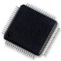
MB91F669PMC-G-JNE1 Fujitsu, MB91F669PMC-G-JNE1 Datasheet - Page 6

MB91F669PMC-G-JNE1
Manufacturer Part Number
MB91F669PMC-G-JNE1
Description
MCU, 32BIT, FR80, 128K FLASH, 64LQFP
Manufacturer
Fujitsu
Datasheet
1.MB91F668PMC-G-JNE1.pdf
(104 pages)
Specifications of MB91F669PMC-G-JNE1
No. Of I/o's
50
Ram Memory Size
16KB
Cpu Speed
33MHz
No. Of Timers
1
No. Of Pwm Channels
4
Digital Ic Case
RoHS Compliant
Core Size
32bit
Program Memory Size
128KB
Oscillator Type
Internal, External
Controller Family/series
MB91665
Rohs Compliant
Yes
- Current page: 6 of 104
- Download datasheet (4Mb)
MB91665 Series
6
■ PIN ASSIGNMENT
LQFP-64 (MB91F669)
Note : The number after the underscore (“_”) in pin names such as XXX_1 and XXX_2 indicates the port number.
P22/A02/TIOA0_1/A18 (5V tolerance,OD)
P20/A00/TMO1_1/A16 (5V tolerance,OD)
P21/A01/TMO2_1/A17 (5V tolerance,OD)
P12/D10/SCK2/INT2 (5V tolerance,OD)
P23/A03/TIOB0_1/A19 (5V tolerance)
P11/D09/SIN2/INT1 (5V tolerance)
For these pins, there are multiple pins that provide the same function for the same channel. Use the
extended port function register (EPFR) to select the pin.
PH3/INT3_1 (5V tolerance)
P14/D12/AIN1/INT4/OUT4
P15/D13/BIN1/INT5/OUT5
P16/D14/ZIN1/INT6/OUT6
P17/D15/INT7/OUT7
P13/D11/INT3
UDM
UDP
Vcc
Vss
10
11
12
13
14
15
16
1
2
3
4
5
6
7
8
9
(FPT-64P-M24)
(TOP VIEW)
LQFP-64
* : Explanation of ( )
5 V tolerance: 5 V tolerant pin
OD: Open drain control pin
48
47
46
45
44
43
42
41
40
39
38
37
36
35
34
33
AVss
P57/WR1/TIOB3_1/TMI2_1
P56/WR0/ZIN1_1/FRCK0/SCK6
P55/RD/BIN1_1/ADTRG0/SIN6
P54/AS/AIN1_1/SOUT6
P53/CS3/FRCK1/TIOA3_1/SCK1_1
P52/CS2/TIOB2_1/SIN1_1
P51/CS1/TIOA2_1/SOUT1_1
P50/CS0/TMO0_1
P07/D07/TIOB3/IN7
P06/D06/TIOA3/SCK1/IN6 (5V tolerance,OD)
P05/D05/TIOB2/SIN1/IN5 (5V tolerance)
P04/D04/TIOA2/SOUT1/IN4 (5V tolerance,OD)
P03/D03/TIOB1/IN3
P02/D02/TIOA1/SCK0_1/IN2 (5V tolerance,OD)
Vcc
DS07-16916-2E
Related parts for MB91F669PMC-G-JNE1
Image
Part Number
Description
Manufacturer
Datasheet
Request
R

Part Number:
Description:
Fujitsu Media Devices Limited [NMOS 1- CHANNEL, 13-BIT AND 3-CHANNEL, 6-BIT D/A CONVERTER]
Manufacturer:
Fujitsu
Datasheet:

Part Number:
Description:
Fujitsu Media Devices Limited [32-bit RISC Microcontroller]
Manufacturer:
Fujitsu
Datasheet:

Part Number:
Description:
Fujitsu Media Devices Limited [MOS 262,144 BIT DYNAMIC RANDOM ACCESS MEMORY]
Manufacturer:
Fujitsu
Datasheet:

Part Number:
Description:
Fujitsu Media Devices Limited [PROGRAMMABLE TIMER]
Manufacturer:
Fujitsu
Datasheet:

Part Number:
Description:
Fujitsu Media Devices Limited [MOS Universal Asynchronous receiver/transmitter(UART)]
Manufacturer:
Fujitsu
Datasheet:

Part Number:
Description:
Fujitsu Media Devices Limited [16M (2M X 8/1M X 16) BIT]
Manufacturer:
Fujitsu
Datasheet:

Part Number:
Description:
KIT, STARTER, MB95200/210/220
Manufacturer:
Fujitsu
Datasheet:

Part Number:
Description:
SWITCHING REGULATOR CONTROLLER
Manufacturer:
Fujitsu
Datasheet:

Part Number:
Description:
QUAD OPERATIONAL AMPLIFIER
Manufacturer:
Fujitsu
Datasheet:

Part Number:
Description:
Switching Regulator Controller (Switchable between push-pull and single-end functions)
Manufacturer:
Fujitsu
Datasheet:

Part Number:
Description:
HIGH-SPEED CMOS SINGLE CHIP 4-BIT MICROCOMPUTER MB88505HHIGH-SPEED CMOS SINGLE CHIP 4-BIT MICROCOMPUTER
Manufacturer:
Fujitsu
Datasheet:

Part Number:
Description:
MOS 1024 BIT NON VOLATILE RANDOM ACCESS MEMORY
Manufacturer:
Fujitsu
Datasheet:

Part Number:
Description:
Schottky TTL 2048-Bit Bipolar Programmable Read-Only Memory
Manufacturer:
Fujitsu
Datasheet:

Part Number:
Description:
QUAD COMPARATOR
Manufacturer:
Fujitsu
Datasheet:


