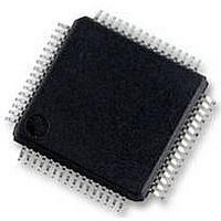
MB91F669PMC-G-JNE1 Fujitsu, MB91F669PMC-G-JNE1 Datasheet - Page 94

MB91F669PMC-G-JNE1
Manufacturer Part Number
MB91F669PMC-G-JNE1
Description
MCU, 32BIT, FR80, 128K FLASH, 64LQFP
Manufacturer
Fujitsu
Datasheet
1.MB91F668PMC-G-JNE1.pdf
(104 pages)
Specifications of MB91F669PMC-G-JNE1
No. Of I/o's
50
Ram Memory Size
16KB
Cpu Speed
33MHz
No. Of Timers
1
No. Of Pwm Channels
4
Digital Ic Case
RoHS Compliant
Core Size
32bit
Program Memory Size
128KB
Oscillator Type
Internal, External
Controller Family/series
MB91665
Rohs Compliant
Yes
- Current page: 94 of 104
- Download datasheet (4Mb)
MB91665 Series
94
*2 : Use differential-Receiver to receive USB differential data signal.
*3 : The output drive capability of the driver is below 0.3 [V] at Low-State (V
*4 : The cross voltage of the external differential output signal (D /D ) of USB I/O buffer is within 1.3 [V] to 2.0 [V].
*5 : Regarding t
Differential-Receiver has 200 [mV] of differential input sensitivity when the differential data input is within 0.8 [V]
Above voltage range is the common mode input voltage range.
2.8 [V] or above (to the V
They indicate rise time (Trise) and fall time (Tfall) of the differential data signal.
They are defined by the time between 10 to 90 of the output signal voltage.
For full-speed buffer, t
to 2.5 [V] to the local ground reference level.
FR
, t
FF
, t
RFM
UDP
UDM
D+
FR
D-
Max 2.0 [V]
Min 1.3 [V]
/t
FF
SS
1.0 [V]
0.2 [V]
ratio is regulated as within 10 to minimize RFI emission.
and 15 k load) at High-State (V
V
CRS
10%
Rise time
t
FR
Common mode input voltage [V]
0.8 [V]
90%
OH
).
90%
Fall time
t
FF
OL
) (to 3.6 [V] and 1.5 k load), and
10%
2.5 [V]
V
CRS
standard range
DS07-16916-2E
(Continued)
Related parts for MB91F669PMC-G-JNE1
Image
Part Number
Description
Manufacturer
Datasheet
Request
R

Part Number:
Description:
Fujitsu Media Devices Limited [NMOS 1- CHANNEL, 13-BIT AND 3-CHANNEL, 6-BIT D/A CONVERTER]
Manufacturer:
Fujitsu
Datasheet:

Part Number:
Description:
Fujitsu Media Devices Limited [32-bit RISC Microcontroller]
Manufacturer:
Fujitsu
Datasheet:

Part Number:
Description:
Fujitsu Media Devices Limited [MOS 262,144 BIT DYNAMIC RANDOM ACCESS MEMORY]
Manufacturer:
Fujitsu
Datasheet:

Part Number:
Description:
Fujitsu Media Devices Limited [PROGRAMMABLE TIMER]
Manufacturer:
Fujitsu
Datasheet:

Part Number:
Description:
Fujitsu Media Devices Limited [MOS Universal Asynchronous receiver/transmitter(UART)]
Manufacturer:
Fujitsu
Datasheet:

Part Number:
Description:
Fujitsu Media Devices Limited [16M (2M X 8/1M X 16) BIT]
Manufacturer:
Fujitsu
Datasheet:

Part Number:
Description:
KIT, STARTER, MB95200/210/220
Manufacturer:
Fujitsu
Datasheet:

Part Number:
Description:
SWITCHING REGULATOR CONTROLLER
Manufacturer:
Fujitsu
Datasheet:

Part Number:
Description:
QUAD OPERATIONAL AMPLIFIER
Manufacturer:
Fujitsu
Datasheet:

Part Number:
Description:
Switching Regulator Controller (Switchable between push-pull and single-end functions)
Manufacturer:
Fujitsu
Datasheet:

Part Number:
Description:
HIGH-SPEED CMOS SINGLE CHIP 4-BIT MICROCOMPUTER MB88505HHIGH-SPEED CMOS SINGLE CHIP 4-BIT MICROCOMPUTER
Manufacturer:
Fujitsu
Datasheet:

Part Number:
Description:
MOS 1024 BIT NON VOLATILE RANDOM ACCESS MEMORY
Manufacturer:
Fujitsu
Datasheet:

Part Number:
Description:
Schottky TTL 2048-Bit Bipolar Programmable Read-Only Memory
Manufacturer:
Fujitsu
Datasheet:

Part Number:
Description:
QUAD COMPARATOR
Manufacturer:
Fujitsu
Datasheet:


