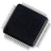
MB91F669PMC-G-JNE1 Fujitsu, MB91F669PMC-G-JNE1 Datasheet - Page 30

MB91F669PMC-G-JNE1
Manufacturer Part Number
MB91F669PMC-G-JNE1
Description
MCU, 32BIT, FR80, 128K FLASH, 64LQFP
Manufacturer
Fujitsu
Datasheet
1.MB91F668PMC-G-JNE1.pdf
(104 pages)
Specifications of MB91F669PMC-G-JNE1
No. Of I/o's
50
Ram Memory Size
16KB
Cpu Speed
33MHz
No. Of Timers
1
No. Of Pwm Channels
4
Digital Ic Case
RoHS Compliant
Core Size
32bit
Program Memory Size
128KB
Oscillator Type
Internal, External
Controller Family/series
MB91665
Rohs Compliant
Yes
- Current page: 30 of 104
- Download datasheet (4Mb)
MB91665 Series
30
■ I/O MAP
[How to read the table]
Notes : When performing a data access, the addresses should be as below.
0000 003C
0000 0000
0000 0040
Address
Do not access the reserved areas.
- Word access : Address should be multiples of 4 (least significant 2 bits should be “00
- Half word access : Address should be multiples of 2 (least significant bit should be “0
- Byte access :
H
H
H
EIRR0 [R/W] B, H, W
PDR0 [R/W] B, H
WDTCR0 [R/W]
XXXXXXXX
- 0 - - 0000
000 0000
B, H
0
WDTCPR0 [R/W]
PDR1 [R/W] B, H
Access unit
Read/write attribute
“
“
“
Register name
at address 4 n
Leftmost register address
register is the MSB of the data.
Initial value after reset
“1” : Initial value“1”
“0” : Initial value“0”
“X” : Initial value undefined
“ - ” : Reserved bit or undefined bit
(
ENIR0 [R/W]
R
R/W
W
B
XXXXXXXX
00000000
00000000
”
”
:
B, H, W
byte
B, H
” :
1
:
:
Indicates that there is a read only bit.
Indicates that there is a read/write bit.
Indicates that there is a write only bit.
,
H
:
Register
half word
(
column 1 of the register is at address 4n, column 2 is
2...
PDR2 [R/W] B, H
XXXXXXXXXXX
)
,
W
2
ELVR0 [R/W] B, H, W
:
(
00000000 00000000
word
For word-length access, column 1 of the
)
)
: Reserved area
PDR3 [R/W] B, H
XXXXXXXX
3
B
B
Watchdog
”)
”)
Port data
DS07-16916-2E
External
interrupt
register
Block
0 to 7
timer
Related parts for MB91F669PMC-G-JNE1
Image
Part Number
Description
Manufacturer
Datasheet
Request
R

Part Number:
Description:
Fujitsu Media Devices Limited [NMOS 1- CHANNEL, 13-BIT AND 3-CHANNEL, 6-BIT D/A CONVERTER]
Manufacturer:
Fujitsu
Datasheet:

Part Number:
Description:
Fujitsu Media Devices Limited [32-bit RISC Microcontroller]
Manufacturer:
Fujitsu
Datasheet:

Part Number:
Description:
Fujitsu Media Devices Limited [MOS 262,144 BIT DYNAMIC RANDOM ACCESS MEMORY]
Manufacturer:
Fujitsu
Datasheet:

Part Number:
Description:
Fujitsu Media Devices Limited [PROGRAMMABLE TIMER]
Manufacturer:
Fujitsu
Datasheet:

Part Number:
Description:
Fujitsu Media Devices Limited [MOS Universal Asynchronous receiver/transmitter(UART)]
Manufacturer:
Fujitsu
Datasheet:

Part Number:
Description:
Fujitsu Media Devices Limited [16M (2M X 8/1M X 16) BIT]
Manufacturer:
Fujitsu
Datasheet:

Part Number:
Description:
KIT, STARTER, MB95200/210/220
Manufacturer:
Fujitsu
Datasheet:

Part Number:
Description:
SWITCHING REGULATOR CONTROLLER
Manufacturer:
Fujitsu
Datasheet:

Part Number:
Description:
QUAD OPERATIONAL AMPLIFIER
Manufacturer:
Fujitsu
Datasheet:

Part Number:
Description:
Switching Regulator Controller (Switchable between push-pull and single-end functions)
Manufacturer:
Fujitsu
Datasheet:

Part Number:
Description:
HIGH-SPEED CMOS SINGLE CHIP 4-BIT MICROCOMPUTER MB88505HHIGH-SPEED CMOS SINGLE CHIP 4-BIT MICROCOMPUTER
Manufacturer:
Fujitsu
Datasheet:

Part Number:
Description:
MOS 1024 BIT NON VOLATILE RANDOM ACCESS MEMORY
Manufacturer:
Fujitsu
Datasheet:

Part Number:
Description:
Schottky TTL 2048-Bit Bipolar Programmable Read-Only Memory
Manufacturer:
Fujitsu
Datasheet:

Part Number:
Description:
QUAD COMPARATOR
Manufacturer:
Fujitsu
Datasheet:


