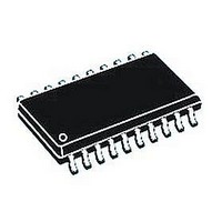
MB95F264KPF-G-SNE2 Fujitsu, MB95F264KPF-G-SNE2 Datasheet - Page 48

MB95F264KPF-G-SNE2
Manufacturer Part Number
MB95F264KPF-G-SNE2
Description
MCU, 8BIT, 20K FLASH, 8FX, 20SOP
Manufacturer
Fujitsu
Datasheet
1.MB95F264KPF-G-SNE2.pdf
(92 pages)
Specifications of MB95F264KPF-G-SNE2
No. Of I/o's
17
Ram Memory Size
496Byte
Cpu Speed
16.25MHz
No. Of Timers
1
No. Of Pwm Channels
2
Core Size
8bit
Program Memory Size
20KB
Oscillator Type
Internal, External
Controller Family/series
MB95260H
Available stocks
Company
Part Number
Manufacturer
Quantity
Price
Company:
Part Number:
MB95F264KPF-G-SNE2
Manufacturer:
Fujitsu
Quantity:
500
MB95260H/270H/280H Series
2. Recommended Operating Conditions
*1: The value varies depending on the operating frequency, the machine clock and the analog guaranteed range.
*2: The value is 2.88 V when the low-voltage detection reset is used.
*3: Use a ceramic capacitor or a capacitor with equivalent frequency characteristics. The bypass capacitor for
WARNING: The recommended operating conditions are required in order to ensure the normal operation of
48
Power supply
voltage
Smoothing
capacitor
Operating
temperature
Parameter
the V
the diagram below. To prevent the device from unintentionally entering an unknown mode due to noise,
minimize the distance between the C pin and C
the layout of a printed circuit board.
• DBG / RST / C pins connection diagram
CC
pin must have a capacitance larger than C
the semiconductor device. All of the device's electrical characteristics are warranted when the
device is operated within these ranges.
Always use semiconductor devices within their recommended operating condition ranges.
Operation outside these ranges may adversely affect reliability and could result in device failure.
No warranty is made with respect to uses, operating conditions, or combinations not represented
on the data sheet. Users considering application outside the listed conditions are advised to contact
their representatives beforehand.
Symbol
V
C
T
CC
A
S
2.4*
*:
0.022
Min
2.3
2.9
2.3
-40
Since the DBG pin becomes a communication pin in on-chip debug mode,
set a pull-up resistor value suiting the input/output specifications of P12/DBG.
+ 5
1
*
Value
2
Cs
5.5*
Max
+ 85
+ 35
5.5
5.5
5.5
1
1
Unit
µF *3
°C
V
S
C
and the distance between C
In normal operation
Hold condition in stop mode
In normal operation
Hold condition in stop mode
Other than on-chip debug mode
On-chip debug mode
S
. For the connection to a smoothing capacitor C
DBG
RST
Remarks
S
and the V
Other than on-chip debug
mode
On-chip debug mode
*
SS
pin when designing
DS07–12627–6E
(V
SS
= 0.0 V)
S
, see


