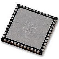
LTC3675EUFF#PBF Linear Technology, LTC3675EUFF#PBF Datasheet - Page 14

LTC3675EUFF#PBF
Manufacturer Part Number
LTC3675EUFF#PBF
Description
IC, PMIC, 1A, QFN-44
Manufacturer
Linear Technology
Datasheet
1.LTC3675EUFFPBF.pdf
(36 pages)
Specifications of LTC3675EUFF#PBF
Supply Voltage
5.5V
No. Of Step-down Dc - Dc Converters
4
No. Of Ldo Regulators
1
Digital Ic Case Style
QFN
No. Of Pins
44
No. Of Regulated Outputs
7
Operating Temperature Range
-40°C To +125°C
Rohs Compliant
Yes
Lead Free Status / RoHS Status
Lead free / RoHS Compliant
Available stocks
Company
Part Number
Manufacturer
Quantity
Price
PIN FUNCTIONS
LTC3675
EN1 (Pin 1): Buck Regulator 1 Enable Input. Active
high.
FB1 (Pin 2): Buck Regulator 1 Feedback Pin. Receives feed-
back by a resistor divider connected across the output.
FB2 (Pin 3): Buck Regulator 2 Feedback Pin. Receives
feedback by a resistor divider connected across the output.
Connecting FB2 to V
buck regulator 1 for higher current.
EN2 (Pin 4): Buck Regulator 2 Enable Input. Active
high.
SW1 (Pin 5): Buck Regulator 1 Switch Node. External
inductor connects to this pin.
V
pling capacitor to GND is recommended. Must be connected
to all other V
V
pling capacitor to GND is recommended. Must be connected
to all other V
SW2 (Pin 8): Buck Regulator 2 Switch Node. External
inductor connects to this pin.
SW3 (Pin 9): Buck Regulator 3 Switch Node. External
inductor connects to this pin.
V
10μF decoupling capacitor to GND is recommended.
Must be connected to all other V
7, 31, 34, 40).
SW4 (Pin 11): Buck Regulator 4 Switch Node. External
inductor connects to this pin.
EN3 (Pin 12): Buck Regulator 3 Enable Input. Active
high.
14
IN
IN
IN
(Pin 6): Buck Regulator 1 Input Supply. A 10μF decou-
(Pin 7): Buck Regulator 2 Input Supply. A 10μF decou-
(Pin 10): Buck Regulators 3 and 4 Input Supply. A
IN
IN
supply pins (Pins 7, 10, 31, 34, 40).
supply pins (Pins 6, 10, 31, 34, 40).
IN
combines buck regulator 2 with
IN
supply pins (Pins 6,
EN4 (Pin 13): Buck Regulator 4 Enable Input. Active
high.
FB4 (Pin 14): Buck Regulator 4 Feedback Pin. Receives
feedback by a resistor divider connected across the output.
Connecting FB4 to V
buck regulator 3 for higher current.
FB3 (Pin 15): Buck Regulator 3 Feedback Pin. Receives
feedback by a resistor divider connected across the output.
Connecting FB3 to V
buck regulator 2 for higher current.
LED_OV (Pin 16): Overvoltage Protection Pin for LED
Driver.
LED1 (Pin 17): Connect a string of up to 10 LEDs to this
pin.
SW7 (Pins 18, 19, 20): LED Driver Switch Node. External
inductor connects to these pins.
LED2 (Pin 21): Connect a string of up to 10 LEDs to this
pin.
CT (Pin 22): Timing Capacitor Pin. A capacitor connected
to GND sets a time constant which is scaled for use by
the WAKE, RSTB and IRQB pins.
RSTB (Pin 23): Reset Pin. Open drain output. When the
regulated output voltage of any enabled switching regula-
tor is more than 6.5% below its programmed level, this
pin is driven LOW. Assertion delay is scaled by the C
capacitor.
IRQB (Pin 24): Interrupt Pin. Open drain output. When
undervoltage, overtemperature, or an unmasked error
condition is detected, this pin is driven LOW. Assertion
delay is scaled by the C
IN
IN
T
combines buck regulator 4 with
combines buck regulator 3 with
capacitor.
3675f
T


