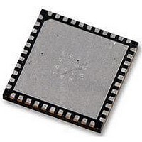
LTC3675EUFF#PBF Linear Technology, LTC3675EUFF#PBF Datasheet - Page 17

LTC3675EUFF#PBF
Manufacturer Part Number
LTC3675EUFF#PBF
Description
IC, PMIC, 1A, QFN-44
Manufacturer
Linear Technology
Datasheet
1.LTC3675EUFFPBF.pdf
(36 pages)
Specifications of LTC3675EUFF#PBF
Supply Voltage
5.5V
No. Of Step-down Dc - Dc Converters
4
No. Of Ldo Regulators
1
Digital Ic Case Style
QFN
No. Of Pins
44
No. Of Regulated Outputs
7
Operating Temperature Range
-40°C To +125°C
Rohs Compliant
Yes
Lead Free Status / RoHS Status
Lead free / RoHS Compliant
Available stocks
Company
Part Number
Manufacturer
Quantity
Price
OPERATION
The LTC3675 has six monolithic synchronous switching
regulators and a dual string boost LED driver and is designed
to operate from a single Li-Ion battery. All of the switching
regulators and the LED driver are internally compensated
and need only external feedback resistors for regulation.
The switching regulators also offer two operating modes:
Burst Mode operation for higher effi ciency at light loads
and pulse-skipping/PWM mode. In Burst Mode operation
at light loads, the output capacitor is charged to a voltage
slightly higher than its regulation point. The regulator then
goes into sleep, during which the output capacitor provides
the load current. In sleep most of the regulator’s circuitry
is powered down, helping conserve battery power. When
the output capacitor droops below its programmed value,
the circuitry is powered on and another burst cycle begins.
The sleep time decreases as load current increases.
All switching regulators and LED driver may be confi gured
via I
LTC3675 in the most effi cient manner. I
also be read back via the I
was not corrupted during a transmission.
All the regulators can be enabled via I
buck regulators and the buck-boost regulator may also be
enabled via enable pins. The enable pins have two different
enable threshold voltages that depend on the operating
state of the LTC3675. With all regulators disabled, the en-
able pin threshold is at 650mV. If any regulator is enabled
either by its enable pin or an I
able pin thresholds are at 400mV. A precision comparator
detects a voltage greater than 400mV on the enable pin
and turns that regulator on. This precision threshold may
be used to sequentially enable regulators. If all regulators
are disabled, all the command registers are set in their
default state.
There are also 2 bytes of data that report any fault condi-
tions on the LTC3675 via I
BUCK SWITCHING REGULATOR
The LTC3675 contains four buck regulators. Two of the
buck regulators are designed to deliver up to 1A load
current each while the other two regulators can deliver
up to 500mA each.
2
C, providing the user with the fl exibility to operate the
2
2
C port, to ensure a command
C read back.
2
C command, then the en-
2
2
C commands. The
C commands can
The buck regulators can operate in either of two modes. In
pulse-skipping mode, the regulator will skip pulses at light
loads but will operate at a constant frequency of 2.25MHz
at higher loads. In Burst Mode operation, the regulator will
burst at light loads whereas at higher loads it will operate
at constant frequency PWM mode of operation, much the
same as pulse-skipping mode at high load. In shutdown,
an I
SW node in a high impedance state or pull the SW node
to GND through a 10k resistor.
The buck regulators have forward and reverse current
limiting, soft-start to limit inrush current during start-up,
short-circuit protection and slew rate control for lower
radiated EMI.
Each buck regulator may be enabled via its enable pin or
I
age and switch slew rate can all be controlled via I
applications that require higher power, buck regulators
may be combined together.
BUCK REGULATORS WITH COMBINED POWER STAGES
Two adjacent buck regulators may be combined in a
master-slave confi guration by connecting their SW pins
together and connecting the higher numbered buck’s FB
pin to the input supply. The lower numbered buck is always
the master. In Figure 1, buck regulator 1 is the master. The
feedback network connected to the FB1 pin programs the
2
C. The mode of operation, the feedback regulation volt-
V
V
2
IN
IN
C control bit provides the fl exibility to either keep the
Figure 1. Buck Regulators Confi gured as Master-Slave
EN1
EN2
BUCK REGULATOR 1
BUCK REGULATOR 2
(MASTER)
(SLAVE)
SW1
SW2
3675 F01
FB1
FB2
V
IN
L1
400k
800k
LTC3675
C
OUT
17
1.2V
2A
V
2
OUT
C. For
3675f


