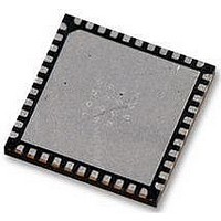
LTC3675EUFF#PBF Linear Technology, LTC3675EUFF#PBF Datasheet - Page 31

LTC3675EUFF#PBF
Manufacturer Part Number
LTC3675EUFF#PBF
Description
IC, PMIC, 1A, QFN-44
Manufacturer
Linear Technology
Datasheet
1.LTC3675EUFFPBF.pdf
(36 pages)
Specifications of LTC3675EUFF#PBF
Supply Voltage
5.5V
No. Of Step-down Dc - Dc Converters
4
No. Of Ldo Regulators
1
Digital Ic Case Style
QFN
No. Of Pins
44
No. Of Regulated Outputs
7
Operating Temperature Range
-40°C To +125°C
Rohs Compliant
Yes
Lead Free Status / RoHS Status
Lead free / RoHS Compliant
Available stocks
Company
Part Number
Manufacturer
Quantity
Price
APPLICATIONS INFORMATION
The sub-address for the latched status register is 0Dh and
its format is as follows:
A write operation cannot be performed to either of the
status registers.
PCB Considerations
When laying out the printed circuit board, the following
list should be followed to ensure proper operation of the
LTC3675:
1. The exposed pad of the package (pin 45) should connect
2. All the input supply pins must be tied together and each
3. The switching regulator input supply pins and their re-
Status Byte Read Back
When either the RSTB or IRQB pin is pulled low, it indicates
to the user that a fault condition has occurred. To fi nd out
the exact nature of the fault, the user can read the status reg-
isters. There are two status registers. One register provides
real time fault condition reporting while a second register
latches data when an interrupt has occurred. Figure 4
shows the operation of the real time and latched status
registers. The contents of the latched status register are
cleared when a CLRINT signal is issued. A PGOOD bit is
a ‘0’ if that regulator’s output voltage is more than 7.5%
below its programmed value.
The sub-address for the real time status register is 0Ch
and its format is as follows:
Unused
directly to a large ground plane to minimize thermal and
electrical impedance.
supply pin should have a decoupling capacitor.
spective decoupling capacitors should be kept as short
as possible. The GND side of these capacitors should
connect directly to the ground plane of the part. These
capacitors provide the AC current to the internal power
MOSFETs and their drivers. It’s important to minimize
inductance from these capacitors to the V
LTC3675.
BIT7
BIT7
UV
Unused
BIT6
BIT6
OT
PGOOD6
PGOOD6
BIT5
BIT5
PGOOD5
PGOOD5
BIT4
BIT4
PGOOD4
PGOOD4
BIT3
BIT3
IN
pins of the
PGOOD3
PGOOD3
BIT2
BIT2
4. The switching power traces connecting SW1, SW2,
5. The GND side of the switching regulator output capaci-
6. In a combined buck regulator application the trace length
PGOOD2
PGOOD2
BIT1
BIT1
SW3, SW4, SW5, SWAB6, SWCD6 and SW7 to their
respective inductors should be minimized to reduce
radiated EMI and parasitic coupling. Due to the large
voltage swing of the switching nodes, high input im-
pedance sensitive nodes such as the feedback nodes
and LED_OV node should be kept far away or shielded
from the switching nodes or poor performance could
result.
tors should connect directly to the thermal ground plane
of the part. Minimize the trace length from the output
capacitor to the inductor(s)/pin(s).
of switch nodes to the inductor must be kept equal to
ensure proper operation.
PGOOD1
PGOOD1
BIT0
BIT0
LTC3675
31
3675f


